 |
Motor de Búsqueda de Datasheet de Componentes Electrónicos |
|
|
Motor de Búsqueda de Datasheet de Componentes Electrónicos |
|
The question interval is too short.
Please try again in a few seconds.

Hello, Please ask a question about AD7008AP20 Datasheet
# Example questions:
➢ What is the reset state of the iqmod register?
➢ What is the source register when tc3-tc0 are x, x, x, x, 0, 0, 0, x, x, 1, 1, 0, 0?
➢ What is the effect of setting cr3 to '1' as described in table iv?
| Part No. | AD7008AP20 |
| Manufacturer | AD |
| Size | 505 Kbytes |
| Pages | 16 pages |
| Description | CMOS DDS Modulator |

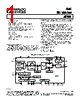


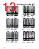
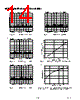
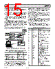
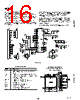

1. Overview: What is the AD7008?
️· CMOS DDS Modulator: The AD7008 is a digital direct-synthesis (DDS) modulator, meaning it creates a precise, programmable waveform based on digital inputs.
️· Flexibility: It's designed for a variety of applications involving amplitude and phase modulation.
2. Key Features & Registers:
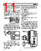
️· Command Register (CR3-CR0): Controls core operating modes. Crucial for initial setup and must be set by the user.
- CR0: Selects 8-bit or 16-bit databus for parallel writes.
- CR1: Enables low-power sleep mode (disables clocks/DAC current sources).
- CR2: Enables/bypasses amplitude modulation (IQ modulation).
- CR3: Enables/disables a synchronization pipeline for control signals (affects latency).
️· Frequency Registers (FREQ0, FREQ1): 32-bit registers. Determine the output frequency by specifying a fraction of the clock frequency.
️· Phase Register: 12-bit. Adds a phase offset to the output waveform.
️· IQ Modulation Register: 20-bit. Defines the amplitude and phase of I and Q signals.
️· Data Busses: D7-D0 and D15-D8 for data input.
3. Operation and Control:
️· Chip Select (CS) and Write (WR): Control parallel writes to the assembly registers.
️· Serial Interface: Uses SCLK and SDATA for serial data input into a serial assembly register.
️· Reset: Resets the command and modulation registers to zero.
️· Sleep Mode: CR1 enables low power operation.
️· Latency: Key parameter influenced by CR3 (synchronizer enable/disable). Pipeline delays vary depending on the operating mode.
4. Tables (Highlights):
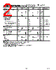
️· Table II (Source/Destination Registers): Describes how TC3-TC0 and LOAD signals control register transfers.
️· Table III (Control Registers): Summarizes the purpose of each bit in the command register.
️· Table IV (Command Register Bits): Detailed descriptions of the bits used in CR0, CR1, CR2 and CR3
5. Important Considerations:
️· Synchronization: The CR3 bit controls whether the control signals (FSELECT, LOAD, TC3-TC0) go through a synchronization pipeline, impacting latency.
️· Command Register Initialization: The command register *must* be initialized by the user before the AD7008 can operate correctly.
️· Parallel Register Access: The parallel assembly register must be written to twice for the 16-bit Databus Access
1. Overview: What is the AD7008?
️· CMOS DDS Modulator: The AD7008 is a digital direct-synthesis (DDS) modulator, meaning it creates a precise, programmable waveform based on digital inputs.
️· Flexibility: It's designed for a variety of applications involving amplitude and phase modulation.
2. Key Features & Registers:
️· Command Register (CR3-CR0): Controls core operating modes. Crucial for initial setup and must be set by the user.
- CR0: Selects 8-bit or 16-bit databus for parallel writes.
- CR1: Enables low-power sleep mode (disables clocks/DAC current sources).
- CR2: Enables/bypasses amplitude modulation (IQ modulation).
- CR3: Enables/disables a synchronization pipeline for control signals (affects latency).
️· Frequency Registers (FREQ0, FREQ1): 32-bit registers. Determine the output frequency by specifying a fraction of the clock frequency.
️· Phase Register: 12-bit. Adds a phase offset to the output waveform.
️· IQ Modulation Register: 20-bit. Defines the amplitude and phase of I and Q signals.
️· Data Busses: D7-D0 and D15-D8 for data input.
3. Operation and Control:
️· Chip Select (CS) and Write (WR): Control parallel writes to the assembly registers.
️· Serial Interface: Uses SCLK and SDATA for serial data input into a serial assembly register.
️· Reset: Resets the command and modulation registers to zero.
️· Sleep Mode: CR1 enables low power operation.
️· Latency: Key parameter influenced by CR3 (synchronizer enable/disable). Pipeline delays vary depending on the operating mode.
4. Tables (Highlights):
️· Table II (Source/Destination Registers): Describes how TC3-TC0 and LOAD signals control register transfers.
️· Table III (Control Registers): Summarizes the purpose of each bit in the command register.
️· Table IV (Command Register Bits): Detailed descriptions of the bits used in CR0, CR1, CR2 and CR3
5. Important Considerations:
️· Synchronization: The CR3 bit controls whether the control signals (FSELECT, LOAD, TC3-TC0) go through a synchronization pipeline, impacting latency.
️· Command Register Initialization: The command register *must* be initialized by the user before the AD7008 can operate correctly.
️· Parallel Register Access: The parallel assembly register must be written to twice for the 16-bit Databus Access
| Part No. | AD7008AP20 |
| Manufacturer | AD |
| Size | 505 Kbytes |
| Pages | 16 pages |
| Description | CMOS DDS Modulator |
| ¿ALLDATASHEET es útil para Ud.? [ DONATE ] |
Todo acerca de Alldatasheet | Publicidad | Contáctenos | Política de Privacidad | Enlace a la hoja de datos | Intercambio de Enlaces | Lista de Fabricantes All Rights Reserved©Alldatasheet.com |
| Russian : Alldatasheetru.com | Korean : Alldatasheet.co.kr | Spanish : Alldatasheet.es | French : Alldatasheet.fr | Italian : Alldatasheetit.com Portuguese : Alldatasheetpt.com | Polish : Alldatasheet.pl | Vietnamese : Alldatasheet.vn Indian : Alldatasheet.in | Mexican : Alldatasheet.com.mx | British : Alldatasheet.co.uk | New Zealand : Alldatasheet.co.nz |
|
Family Site : ic2ic.com |
icmetro.com |
 Mexican ▼
  English
 Chinese
 German
 Japanese
 Russian
 Korean
 Spanish
 French
 Italian
 Portuguese
 Polish
 Vietnamese
 Indian
 British
 New Zealand