 |
Motor de Búsqueda de Datasheet de Componentes Electrónicos |
|
|
Motor de Búsqueda de Datasheet de Componentes Electrónicos |
|
The question interval is too short.
Please try again in a few seconds.

Hello, Please ask a question about PIC12C671T Datasheet
# Example questions:
➢ How does the document describe the relationship between the two data memory banks and the rp0 bit?
➢ Explain how the instruction pipeline functions, and what happens if a 'goto' instruction is encountered.
➢ What is the function of the pclath register?
| Part No. | PIC12C671T |
| Manufacturer | MICROCHIP |
| Size | 1Mb |
| Pages | 130 pages |
| Description | 8-Pin, 8-Bit CMOS Microcontroller with A/D Converter and EEPROM Data Memory |


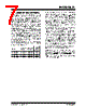


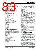


This is a very detailed and comprehensive datasheet excerpt for the PIC12C67X microcontroller. Here's a breakdown of the information presented and its significance:
1. Core Features and Overview:
️· Architecture: Describes the PIC12C67X as part of the PIC microcontroller family.
️· Clocking & Instruction Cycle: Explains the internal clock system using a four-phase clock (Q1-Q4) and how this facilitates a pipelined instruction execution. This pipelining allows the CPU to fetch the next instruction while executing the current one, improving overall performance. The example (Example 2-1) clarifies how instructions are fetched and executed sequentially.
️· Memory Organization: This section lays out how program memory and data memory are structured and addressed. Crucially, it describes the "wrap-around" behavior if code attempts to access program memory beyond the physically implemented space.
️· Bank Switching: Introduces the concept of bank switching using the RP0 bit in the STATUS register. This allows the microcontroller to access more general-purpose registers than would be available in a single bank.
️· Special Function Registers (SFRs): Describes how these registers provide control and configuration options for the microcontroller's internal peripherals and core functions.
2. Specific Details:
️· Program Memory:
- 13-bit program counter (PC): Allows addressing up to 8192 bytes (8K) of program memory.
- Memory Map: Specifies the address ranges for PIC12C671 and PIC12C672 models. Addresses beyond these ranges wrap around.
- Reset and Interrupt Vectors: Highlights the specific memory addresses used for jump to reset and interrupt routines.
️· Data Memory:
- Bank 0 and Bank 1: The microcontroller's RAM is divided into two banks.
- RP0: Bank Select Bit – controls which bank is active.
- Special Function Registers (SFRs) are located in both banks.
- Common SFRs are mirrored in both banks for faster access.
️· Register File:
- Contains General Purpose Registers (GPRs) and Special Function Registers (SFRs).
️· Clocking Scheme: Explains the internal clocking mechanism.
️· Instruction Cycle: Details the four-phase instruction cycle (Q1-Q4).
️· Pipelining: Illustrates the pipelined instruction execution, which improves overall performance.
️· Peripheral Module Information: Hints at the existence of peripheral modules (timers, ADC, etc.) without delving into specifics.
3. Key Technical Insights & Implications:
️· Addressable Space: Understanding the limited addressable space (especially for the PIC12C671) is vital for code development.
️· Bank Switching: Bank switching is a key feature for maximizing the use of limited RAM.
️· SFR Mirroring: Reduces code size and improves access speed to frequently used registers.
️· Pipelined Execution: This feature contributes to the microcontroller’s performance by overlapping instruction fetch and execution.
️· Clocking and Reset: Important for proper operation and debugging.
️· Interrupt Vectors: Indicates the exact locations in memory for jump to interrupt routines.
4. Limitations and Assumptions (Based on the Excerpt):
️· Peripheral Details: This excerpt focuses on architecture, memory, and the basics of operation. The specifics of each peripheral module (timers, ADC, etc.) are not discussed.
️· Full Datasheet Required: This is just a portion of the full datasheet. More detailed information is necessary for complete device understanding.
This excerpt provides a foundational understanding of the PIC12C67X's architecture and organization, setting the stage for deeper exploration of its features and capabilities.
This is a very detailed and comprehensive datasheet excerpt for the PIC12C67X microcontroller. Here's a breakdown of the information presented and its significance:
1. Core Features and Overview:
️· Architecture: Describes the PIC12C67X as part of the PIC microcontroller family.
️· Clocking & Instruction Cycle: Explains the internal clock system using a four-phase clock (Q1-Q4) and how this facilitates a pipelined instruction execution. This pipelining allows the CPU to fetch the next instruction while executing the current one, improving overall performance. The example (Example 2-1) clarifies how instructions are fetched and executed sequentially.
️· Memory Organization: This section lays out how program memory and data memory are structured and addressed. Crucially, it describes the "wrap-around" behavior if code attempts to access program memory beyond the physically implemented space.
️· Bank Switching: Introduces the concept of bank switching using the RP0 bit in the STATUS register. This allows the microcontroller to access more general-purpose registers than would be available in a single bank.
️· Special Function Registers (SFRs): Describes how these registers provide control and configuration options for the microcontroller's internal peripherals and core functions.
2. Specific Details:
️· Program Memory:
- 13-bit program counter (PC): Allows addressing up to 8192 bytes (8K) of program memory.
- Memory Map: Specifies the address ranges for PIC12C671 and PIC12C672 models. Addresses beyond these ranges wrap around.
- Reset and Interrupt Vectors: Highlights the specific memory addresses used for jump to reset and interrupt routines.
️· Data Memory:
- Bank 0 and Bank 1: The microcontroller's RAM is divided into two banks.
- RP0: Bank Select Bit – controls which bank is active.
- Special Function Registers (SFRs) are located in both banks.
- Common SFRs are mirrored in both banks for faster access.
️· Register File:
- Contains General Purpose Registers (GPRs) and Special Function Registers (SFRs).
️· Clocking Scheme: Explains the internal clocking mechanism.
️· Instruction Cycle: Details the four-phase instruction cycle (Q1-Q4).
️· Pipelining: Illustrates the pipelined instruction execution, which improves overall performance.
️· Peripheral Module Information: Hints at the existence of peripheral modules (timers, ADC, etc.) without delving into specifics.
3. Key Technical Insights & Implications:
️· Addressable Space: Understanding the limited addressable space (especially for the PIC12C671) is vital for code development.
️· Bank Switching: Bank switching is a key feature for maximizing the use of limited RAM.
️· SFR Mirroring: Reduces code size and improves access speed to frequently used registers.
️· Pipelined Execution: This feature contributes to the microcontroller’s performance by overlapping instruction fetch and execution.
️· Clocking and Reset: Important for proper operation and debugging.
️· Interrupt Vectors: Indicates the exact locations in memory for jump to interrupt routines.
4. Limitations and Assumptions (Based on the Excerpt):
️· Peripheral Details: This excerpt focuses on architecture, memory, and the basics of operation. The specifics of each peripheral module (timers, ADC, etc.) are not discussed.
️· Full Datasheet Required: This is just a portion of the full datasheet. More detailed information is necessary for complete device understanding.
This excerpt provides a foundational understanding of the PIC12C67X's architecture and organization, setting the stage for deeper exploration of its features and capabilities.
| Part No. | PIC12C671T |
| Manufacturer | MICROCHIP |
| Size | 1Mb |
| Pages | 130 pages |
| Description | 8-Pin, 8-Bit CMOS Microcontroller with A/D Converter and EEPROM Data Memory |
| ¿ALLDATASHEET es útil para Ud.? [ DONATE ] |
Todo acerca de Alldatasheet | Publicidad | Contáctenos | Política de Privacidad | Enlace a la hoja de datos | Intercambio de Enlaces | Lista de Fabricantes All Rights Reserved©Alldatasheet.com |
| Russian : Alldatasheetru.com | Korean : Alldatasheet.co.kr | Spanish : Alldatasheet.es | French : Alldatasheet.fr | Italian : Alldatasheetit.com Portuguese : Alldatasheetpt.com | Polish : Alldatasheet.pl | Vietnamese : Alldatasheet.vn Indian : Alldatasheet.in | Mexican : Alldatasheet.com.mx | British : Alldatasheet.co.uk | New Zealand : Alldatasheet.co.nz |
|
Family Site : ic2ic.com |
icmetro.com |
 Mexican ▼
  English
 Chinese
 German
 Japanese
 Russian
 Korean
 Spanish
 French
 Italian
 Portuguese
 Polish
 Vietnamese
 Indian
 British
 New Zealand