 |
Motor de Búsqueda de Datasheet de Componentes Electrónicos |
|
|
Motor de Búsqueda de Datasheet de Componentes Electrónicos |
|
The question interval is too short.
Please try again in a few seconds.

Hello, Please ask a question about 54150 Datasheet
# Example questions:
➢ For the 'strobe to y' input, what is the range of propagation delays (tplh and tphl)?
➢ What is the difference in maximum propagation delay (tphl) between the 'select (4 levels) to y' input and the 'd0-d7 to w' input?
➢ If rl = 400ω and cl = 15pf, what is the maximum propagation delay time (tphl) from d0-d7 to y?
| Part No. | 54150 |
| Manufacturer | NSC |
| Size | 182 Kbytes |
| Pages | 10 pages |
| Description | Data Selectors/Multiplexers |




Overall Context:
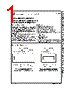
The document details the electrical characteristics and timing performance of a logic device (likely a 8-bit register). It provides specifications to ensure proper operation within a circuit.
Key Sections and Summaries:
1. Initial Timing Characteristics (First Table):
- RL e 400X, CL e 15 pF: This signifies that the timing values are measured under specific load conditions: a load resistance (RL) of 400 ohms and a capacitance (CL) of 15 picofarads. This is a standard way to normalize timing specifications, so they can be compared across different devices.
- Select to Y & Select to W: The device has input signals labeled 'Select' that control how the output 'Y' and 'W' behave. The timings specify delays related to those selections.
- D0-D7 to Y & D0-D7 to W: These timings describe the propagation delay (time for a signal to travel through the logic) for data signals (D0 through D7) reaching outputs 'Y' and 'W'.
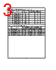
2. Second Set of Timing Characteristics:
- Similar to the first table, but with different timings. This implies that there may be different operating conditions or configurations being specified.
- Slightly lower timings are specified in this second table compared to the first.
3. Logic Diagrams
- This section would presumably contain visual representations of the internal logic circuitry of the integrated circuit.
Key Data Points (Illustrative, based on fragments):
️· Propagation Delays: The most significant data are the *propagation delays*. These are the critical timings that determine how quickly the output changes in response to changes at the inputs. Delays range from approximately 14ns to 38ns.
️· Load Conditions: The timings are all referenced to an RL of 400 ohms and a CL of 15 pF.
️· Signal Paths: The timings specify delays associated with specific signal paths (Select to Y, Data to Output).
In Simple Terms:
The document tells you how long it takes for different signals to pass through the device, which helps engineers understand its behavior and design reliable circuits.
Overall Context:
The document details the electrical characteristics and timing performance of a logic device (likely a 8-bit register). It provides specifications to ensure proper operation within a circuit.
Key Sections and Summaries:
1. Initial Timing Characteristics (First Table):
- RL e 400X, CL e 15 pF: This signifies that the timing values are measured under specific load conditions: a load resistance (RL) of 400 ohms and a capacitance (CL) of 15 picofarads. This is a standard way to normalize timing specifications, so they can be compared across different devices.
- Select to Y & Select to W: The device has input signals labeled 'Select' that control how the output 'Y' and 'W' behave. The timings specify delays related to those selections.
- D0-D7 to Y & D0-D7 to W: These timings describe the propagation delay (time for a signal to travel through the logic) for data signals (D0 through D7) reaching outputs 'Y' and 'W'.
2. Second Set of Timing Characteristics:
- Similar to the first table, but with different timings. This implies that there may be different operating conditions or configurations being specified.
- Slightly lower timings are specified in this second table compared to the first.
3. Logic Diagrams
- This section would presumably contain visual representations of the internal logic circuitry of the integrated circuit.
Key Data Points (Illustrative, based on fragments):
️· Propagation Delays: The most significant data are the *propagation delays*. These are the critical timings that determine how quickly the output changes in response to changes at the inputs. Delays range from approximately 14ns to 38ns.
️· Load Conditions: The timings are all referenced to an RL of 400 ohms and a CL of 15 pF.
️· Signal Paths: The timings specify delays associated with specific signal paths (Select to Y, Data to Output).
In Simple Terms:
The document tells you how long it takes for different signals to pass through the device, which helps engineers understand its behavior and design reliable circuits.
| Part No. | 54150 |
| Manufacturer | NSC |
| Size | 182 Kbytes |
| Pages | 10 pages |
| Description | Data Selectors/Multiplexers |
| ¿ALLDATASHEET es útil para Ud.? [ DONATE ] |
Todo acerca de Alldatasheet | Publicidad | Contáctenos | Política de Privacidad | Enlace a la hoja de datos | Intercambio de Enlaces | Lista de Fabricantes All Rights Reserved©Alldatasheet.com |
| Russian : Alldatasheetru.com | Korean : Alldatasheet.co.kr | Spanish : Alldatasheet.es | French : Alldatasheet.fr | Italian : Alldatasheetit.com Portuguese : Alldatasheetpt.com | Polish : Alldatasheet.pl | Vietnamese : Alldatasheet.vn Indian : Alldatasheet.in | Mexican : Alldatasheet.com.mx | British : Alldatasheet.co.uk | New Zealand : Alldatasheet.co.nz |
|
Family Site : ic2ic.com |
icmetro.com |
 Mexican ▼
  English
 Chinese
 German
 Japanese
 Russian
 Korean
 Spanish
 French
 Italian
 Portuguese
 Polish
 Vietnamese
 Indian
 British
 New Zealand