 |
Motor de Búsqueda de Datasheet de Componentes Electrónicos |
|
|
Motor de Búsqueda de Datasheet de Componentes Electrónicos |
|
The question interval is too short.
Please try again in a few seconds.

Hello, Please ask a question about NCP4353_15 Datasheet
# Example questions:
➢ The text mentions two divider types for vsns. what condition determines which divider type should be used, and what equation defines this condition?
➢ What components are recommended to be added in series from vout to vcc to reduce voltage spikes and drops, and what are their recommended values?
➢ How does the ncp435x series operate when the output voltage decreases below a set minimum level (excluding ncp4353a)?
| Part No. | NCP4353_15 |
| Manufacturer | ONSEMI |
| Size | 274 Kbytes |
| Pages | 17 pages |
| Description | Secondary Side SMPS OFF Mode Controller |


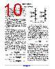


1. General Overview & Series Information
️· Chip Series: NCP435x (likely a family of ICs). Variations include NCP4353A, NCP4353B, and potentially others.
️· Purpose: Designed for voltage regulation (and potentially current regulation, based on "A versions").
️· Application: Primarily intended for use in power supplies with a primary/secondary control architecture (flyback).
2. Electrical Characteristics & Operating Parameters
️· Supply Voltage (VCC): 36V maximum.
️· Operating Voltage Range (VCC): 3.5V (startup) to 2.5V (shutdown).
️· Voltage Regulation Path:
- Output voltage detected on VSNS pin via voltage divider (R4, R5, R6).
- Comparison with internal reference voltage (VREF).
- Transconductance amplifiers (gm V, gm C) provide amplification and drive the FBC (Feedback Controller) or DRIVE pin.
- Compensation network on FBC/DRIVE pin for frequency compensation.
- Optocoupler driven by FBC/DRIVE pin for primary-side regulation.
️· Current Regulation Path (NCP4353A Versions Only):
- Output current sensed by shunt resistor (R12).
- Voltage drop across R12 compared to reference voltage (VREFC)
- Transconductance amplifier (gm C) amplifies the difference and drives FBC/DRIVE.
- Compensation network for current regulation.
3. Application & Component Recommendations
️· RC Filter: Recommended between VOUT and VCC (R1, C3) to reduce voltage spikes. Suggested values: 220Ω and 1µF.
️· VSNS Voltage Divider: Two types (Type 2 and Type 3), selection based on Equation 1 relating VOUT, VREF, and VMIN. Specific formulas provided for output voltage calculation (Equations 2 & 3) depending on divider type.
️· Off-Mode Operation:
- Important for ultra-low/zero output current conditions.
- Minimized power consumption through extended off-times.
- Output voltage fluctuates between nominal and minimum.
- Primary controller is activated when the output voltage drops below the minimum level.
- Based on comparison of output voltage and a fixed resistance network (D2, C2, R8, R9).
4. Key Equations & Relationships
️· Equation 1 (VSNS divider selection): `VOUT = VREF - [R4] / [R5] * [R6]` (This likely has variations based on the divider type)
️· Equation 2 (Output Voltage, Type 1 Divider): `VOUT = VREF - [R4] / [R5] * [R6]`
️· Equation 2 (Output Voltage, Type 3 Divider): `VOUT = VREF - [R4] / [R6] * [R5]`
️· Current Regulation (Equation 3): `I OUTLIM = VREFC / R12`
5. Pins
️· VCC: Supply Voltage
️· VSNS: Voltage Sensing
️· FBC: Feedback Controller
️· DRIVE: Drive Pin
️· ISNS: Current Sensing
️· R4, R5, R6: Components of VSNS voltage divider.
️· R12: Shunt Resistor for Current Sensing
Important Notes:
️· The document is excerpted, so there might be missing context.
️· The term "FBC" is used repeatedly; it likely represents the feedback controller chip/circuit.
️· The "A versions" (e.g., NCP4353A) have current regulation features that are not present in other versions.
️· Pay close attention to the different voltage divider configurations (Type 1, and Type 2), as the calculations and application differ.
1. General Overview & Series Information
️· Chip Series: NCP435x (likely a family of ICs). Variations include NCP4353A, NCP4353B, and potentially others.
️· Purpose: Designed for voltage regulation (and potentially current regulation, based on "A versions").
️· Application: Primarily intended for use in power supplies with a primary/secondary control architecture (flyback).
2. Electrical Characteristics & Operating Parameters
️· Supply Voltage (VCC): 36V maximum.
️· Operating Voltage Range (VCC): 3.5V (startup) to 2.5V (shutdown).
️· Voltage Regulation Path:
- Output voltage detected on VSNS pin via voltage divider (R4, R5, R6).
- Comparison with internal reference voltage (VREF).
- Transconductance amplifiers (gm V, gm C) provide amplification and drive the FBC (Feedback Controller) or DRIVE pin.
- Compensation network on FBC/DRIVE pin for frequency compensation.
- Optocoupler driven by FBC/DRIVE pin for primary-side regulation.
️· Current Regulation Path (NCP4353A Versions Only):
- Output current sensed by shunt resistor (R12).
- Voltage drop across R12 compared to reference voltage (VREFC)
- Transconductance amplifier (gm C) amplifies the difference and drives FBC/DRIVE.
- Compensation network for current regulation.
3. Application & Component Recommendations
️· RC Filter: Recommended between VOUT and VCC (R1, C3) to reduce voltage spikes. Suggested values: 220Ω and 1µF.
️· VSNS Voltage Divider: Two types (Type 2 and Type 3), selection based on Equation 1 relating VOUT, VREF, and VMIN. Specific formulas provided for output voltage calculation (Equations 2 & 3) depending on divider type.
️· Off-Mode Operation:
- Important for ultra-low/zero output current conditions.
- Minimized power consumption through extended off-times.
- Output voltage fluctuates between nominal and minimum.
- Primary controller is activated when the output voltage drops below the minimum level.
- Based on comparison of output voltage and a fixed resistance network (D2, C2, R8, R9).
4. Key Equations & Relationships
️· Equation 1 (VSNS divider selection): `VOUT = VREF - [R4] / [R5] * [R6]` (This likely has variations based on the divider type)
️· Equation 2 (Output Voltage, Type 1 Divider): `VOUT = VREF - [R4] / [R5] * [R6]`
️· Equation 2 (Output Voltage, Type 3 Divider): `VOUT = VREF - [R4] / [R6] * [R5]`
️· Current Regulation (Equation 3): `I OUTLIM = VREFC / R12`
5. Pins
️· VCC: Supply Voltage
️· VSNS: Voltage Sensing
️· FBC: Feedback Controller
️· DRIVE: Drive Pin
️· ISNS: Current Sensing
️· R4, R5, R6: Components of VSNS voltage divider.
️· R12: Shunt Resistor for Current Sensing
Important Notes:
️· The document is excerpted, so there might be missing context.
️· The term "FBC" is used repeatedly; it likely represents the feedback controller chip/circuit.
️· The "A versions" (e.g., NCP4353A) have current regulation features that are not present in other versions.
️· Pay close attention to the different voltage divider configurations (Type 1, and Type 2), as the calculations and application differ.
| Part No. | NCP4353_15 |
| Manufacturer | ONSEMI |
| Size | 274 Kbytes |
| Pages | 17 pages |
| Description | Secondary Side SMPS OFF Mode Controller |
| ¿ALLDATASHEET es útil para Ud.? [ DONATE ] |
Todo acerca de Alldatasheet | Publicidad | Contáctenos | Política de Privacidad | Enlace a la hoja de datos | Intercambio de Enlaces | Lista de Fabricantes All Rights Reserved©Alldatasheet.com |
| Russian : Alldatasheetru.com | Korean : Alldatasheet.co.kr | Spanish : Alldatasheet.es | French : Alldatasheet.fr | Italian : Alldatasheetit.com Portuguese : Alldatasheetpt.com | Polish : Alldatasheet.pl | Vietnamese : Alldatasheet.vn Indian : Alldatasheet.in | Mexican : Alldatasheet.com.mx | British : Alldatasheet.co.uk | New Zealand : Alldatasheet.co.nz |
|
Family Site : ic2ic.com |
icmetro.com |
 Mexican ▼
  English
 Chinese
 German
 Japanese
 Russian
 Korean
 Spanish
 French
 Italian
 Portuguese
 Polish
 Vietnamese
 Indian
 British
 New Zealand