 |
Motor de Búsqueda de Datasheet de Componentes Electrónicos |
|
|
Motor de Búsqueda de Datasheet de Componentes Electrónicos |
|
The question interval is too short.
Please try again in a few seconds.

Hello, Please ask a question about AD9832 Datasheet
# Example questions:
➢ What are the acceptable voltage ranges for avdd and dvdd?
➢ What precautions should be taken when changing the fselect, psel0, and psel1 inputs in relation to the mclk signal?
➢ What should be connected to the comp pin and why?
| Part No. | AD9832 |
| Manufacturer | AD |
| Size | 146 Kbytes |
| Pages | 16 pages |
| Description | CMOS Complete DDS |


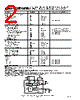


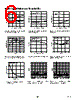


1. Overview:
️· Device: AD9832
️· Type: Direct Digital Synthesis (DDS) device. DDS allows for the generation of precise, programmable waveforms.
️· Key Features (implied from descriptions):
- Programmable Waveform Generation
- Multiple frequency and phase registers
- Digital clock input (MCLK) for precise frequency control
- Serial data interface (SDATA/SCLK) for programming
- Control inputs (FSYNC, FSELECT, PSEL0, PSEL1) for waveform flexibility.
2. Power Supply and Grounding:
️· DVDD: Digital Power Supply (+5V ±10% or +3.3V ±10%) – Requires a 0.1µF decoupling capacitor.
️· DGND: Digital Ground
️· AGND: Analog Ground
️· AVDD: Analog Power Supply (+5V ±10% or +3.3V ±10%) – Requires a 0.1µF decoupling capacitor.
3. Digital Interface & Control Signals:
️· MCLK: Digital Clock Input - Critical for frequency accuracy.
️· SCLK: Serial Clock – Used to clock data into the device.
️· SDATA: Serial Data Input – Carries the waveform data.
️· FSYNC: Data Synchronization Signal - Indicates a new data word is being sent.
️· FSELECT: Frequency Select Input - Chooses which frequency register to use.
️· PSEL0 & PSEL1: Phase Select Inputs – Select which phase register to use.
4. Analog Output & Reference:
️· IOUT: Current Output – This is where the generated waveform is output. Needs a load resistor connected.
️· COMP: Compensation pin for internal reference amplifier. Requires a 10nF decoupling capacitor.
️· REFIN: Voltage Reference input.
️· REFOUT: Voltage Reference output.
5. FS ADJUST:
️· This pin is used in conjunction with a resistor (RSET) to control the full-scale output current. The relationship between the reference voltage (VREFIN) and the full-scale output current (IOUTFULLSCALE) is: IOUTFULLSCALE = 12.5 * VREFIN / RSET.
- RSET is 3.9kΩ when the full scale is in the typical case.
Key Considerations & Best Practices (implied from the descriptions):
️· Decoupling: Proper decoupling capacitors on both digital (DVDD) and analog (AVDD) power supplies are *essential* for stable operation and noise reduction.
️· Clock Stability: The stability and accuracy of MCLK directly impact the generated waveform's frequency accuracy.
️· Signal Integrity: Carefully route signals, especially SCLK and SDATA, to minimize noise and signal reflections.
️· Synchronous Operations: FSELECT and PSEL0/PSEL1 signals need to be stable and well-defined during the MCLK rising edge to avoid unwanted frequency or phase shifts.
️· Reference Voltage: Using a stable reference voltage to REFIN is critical for accurate waveform generation.
In essence, this document provides a foundational understanding of the AD9832's power requirements, control signals, and key output considerations for successful integration.
1. Overview:
️· Device: AD9832
️· Type: Direct Digital Synthesis (DDS) device. DDS allows for the generation of precise, programmable waveforms.
️· Key Features (implied from descriptions):
- Programmable Waveform Generation
- Multiple frequency and phase registers
- Digital clock input (MCLK) for precise frequency control
- Serial data interface (SDATA/SCLK) for programming
- Control inputs (FSYNC, FSELECT, PSEL0, PSEL1) for waveform flexibility.
2. Power Supply and Grounding:
️· DVDD: Digital Power Supply (+5V ±10% or +3.3V ±10%) – Requires a 0.1µF decoupling capacitor.
️· DGND: Digital Ground
️· AGND: Analog Ground
️· AVDD: Analog Power Supply (+5V ±10% or +3.3V ±10%) – Requires a 0.1µF decoupling capacitor.
3. Digital Interface & Control Signals:
️· MCLK: Digital Clock Input - Critical for frequency accuracy.
️· SCLK: Serial Clock – Used to clock data into the device.
️· SDATA: Serial Data Input – Carries the waveform data.
️· FSYNC: Data Synchronization Signal - Indicates a new data word is being sent.
️· FSELECT: Frequency Select Input - Chooses which frequency register to use.
️· PSEL0 & PSEL1: Phase Select Inputs – Select which phase register to use.
4. Analog Output & Reference:
️· IOUT: Current Output – This is where the generated waveform is output. Needs a load resistor connected.
️· COMP: Compensation pin for internal reference amplifier. Requires a 10nF decoupling capacitor.
️· REFIN: Voltage Reference input.
️· REFOUT: Voltage Reference output.
5. FS ADJUST:
️· This pin is used in conjunction with a resistor (RSET) to control the full-scale output current. The relationship between the reference voltage (VREFIN) and the full-scale output current (IOUTFULLSCALE) is: IOUTFULLSCALE = 12.5 * VREFIN / RSET.
- RSET is 3.9kΩ when the full scale is in the typical case.
Key Considerations & Best Practices (implied from the descriptions):
️· Decoupling: Proper decoupling capacitors on both digital (DVDD) and analog (AVDD) power supplies are *essential* for stable operation and noise reduction.
️· Clock Stability: The stability and accuracy of MCLK directly impact the generated waveform's frequency accuracy.
️· Signal Integrity: Carefully route signals, especially SCLK and SDATA, to minimize noise and signal reflections.
️· Synchronous Operations: FSELECT and PSEL0/PSEL1 signals need to be stable and well-defined during the MCLK rising edge to avoid unwanted frequency or phase shifts.
️· Reference Voltage: Using a stable reference voltage to REFIN is critical for accurate waveform generation.
In essence, this document provides a foundational understanding of the AD9832's power requirements, control signals, and key output considerations for successful integration.
| Part No. | AD9832 |
| Manufacturer | AD |
| Size | 146 Kbytes |
| Pages | 16 pages |
| Description | CMOS Complete DDS |
| ¿ALLDATASHEET es útil para Ud.? [ DONATE ] |
Todo acerca de Alldatasheet | Publicidad | Contáctenos | Política de Privacidad | Enlace a la hoja de datos | Intercambio de Enlaces | Lista de Fabricantes All Rights Reserved©Alldatasheet.com |
| Russian : Alldatasheetru.com | Korean : Alldatasheet.co.kr | Spanish : Alldatasheet.es | French : Alldatasheet.fr | Italian : Alldatasheetit.com Portuguese : Alldatasheetpt.com | Polish : Alldatasheet.pl | Vietnamese : Alldatasheet.vn Indian : Alldatasheet.in | Mexican : Alldatasheet.com.mx | British : Alldatasheet.co.uk | New Zealand : Alldatasheet.co.nz |
|
Family Site : ic2ic.com |
icmetro.com |
 Mexican ▼
  English
 Chinese
 German
 Japanese
 Russian
 Korean
 Spanish
 French
 Italian
 Portuguese
 Polish
 Vietnamese
 Indian
 British
 New Zealand