 |
Motor de Búsqueda de Datasheet de Componentes Electrónicos |
|
|
Motor de Búsqueda de Datasheet de Componentes Electrónicos |
|
The question interval is too short.
Please try again in a few seconds.

Hello, Please ask a question about AD9852 Datasheet
# Example questions:
➢ What is the function of the ‘dac rset’ pin (pin 56), and what is the typical range of resistor values that can be used with this pin?
➢ What are the two modes of operation selectable via the ‘s/p select’ pin (pin 71) and what logic level selects each mode?
➢ What is the purpose of the ‘pll filter’ pin (pin 61) and what components are required to connect it properly?
| Part No. | AD9852 |
| Manufacturer | AD |
| Size | 424 Kbytes |
| Pages | 42 pages |
| Description | CMOS 300 MHz Complete-DDS |






1. Device Information:
️· Product: AD9852
️· Type: Programmable Waveform Generator, PLL, and High-Speed Comparator.
️· Key Features:
- Programmable Waveform Generation
- Phase-Locked Loop (PLL)
- High-Speed Comparator
- Supports FSK, BPSK, and Chirp Modes.
- Cosine DAC outputs.
- Analog and Digital supply voltage capabilities.
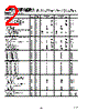
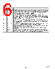
2. Pin Configuration (Key Pins - summarized):
️· DVDD/AVDD/Vdd: Supply voltages (multiple pins)
️· DGND/AGND/GND: Ground pins
️· D0-D7: Digital I/O pins
️· A0-A5: Address/Control pins
️· I/O UD: I/O control.
️· REFCLKB/REFCLK: Reference clock inputs (differential/single-ended).
️· DACBP/DACRSET: DAC bypass capacitor and output current set.
️· MASTER/RESET: Master reset pin for programming bus initialization.
️· S/P SELECT: Serial/Parallel Programming Mode Select.
️· PLL FILTER: PLL filter compensation network.
️· DIFF CLK: Differential Clock Enable
️· VINP/VINN: Comparator Input pins
3. Performance Characteristics (as reflected in the figures):
️· Wideband SFDR (Spurious Free Dynamic Range): Figures 2-7 show SFDR performance across a range of frequencies (19.1 MHz to 119.1 MHz). SFDR values vary with frequency, generally exhibiting good performance within the tested range.
️· Testing Conditions: Reference clock = 30 MHz, REFCLK Multiplier = 10.
4. Figures:
️· The figures illustrate the wideband SFDR (Spurious Free Dynamic Range) performance of the AD9852 at various frequencies (19.1 MHz, 39.1 MHz, 59.1 MHz, 79.1 MHz, 99.1 MHz, 119.1 MHz).
5. Key Points & Cautions:
️· Power Supply: Multiple pins designated for both digital and analog supply voltages. Proper grounding is crucial.
️· PLL Compensation: The PLL filter network requires an external compensation network for optimal performance.
️· Master Reset: A Master Reset is necessary for initialization of the programming bus.
️· SFDR Variation: SFDR is frequency-dependent; see the figures for specific performance at various frequencies.
1. Device Information:
️· Product: AD9852
️· Type: Programmable Waveform Generator, PLL, and High-Speed Comparator.
️· Key Features:
- Programmable Waveform Generation
- Phase-Locked Loop (PLL)
- High-Speed Comparator
- Supports FSK, BPSK, and Chirp Modes.
- Cosine DAC outputs.
- Analog and Digital supply voltage capabilities.
2. Pin Configuration (Key Pins - summarized):
️· DVDD/AVDD/Vdd: Supply voltages (multiple pins)
️· DGND/AGND/GND: Ground pins
️· D0-D7: Digital I/O pins
️· A0-A5: Address/Control pins
️· I/O UD: I/O control.
️· REFCLKB/REFCLK: Reference clock inputs (differential/single-ended).
️· DACBP/DACRSET: DAC bypass capacitor and output current set.
️· MASTER/RESET: Master reset pin for programming bus initialization.
️· S/P SELECT: Serial/Parallel Programming Mode Select.
️· PLL FILTER: PLL filter compensation network.
️· DIFF CLK: Differential Clock Enable
️· VINP/VINN: Comparator Input pins
3. Performance Characteristics (as reflected in the figures):
️· Wideband SFDR (Spurious Free Dynamic Range): Figures 2-7 show SFDR performance across a range of frequencies (19.1 MHz to 119.1 MHz). SFDR values vary with frequency, generally exhibiting good performance within the tested range.
️· Testing Conditions: Reference clock = 30 MHz, REFCLK Multiplier = 10.
4. Figures:
️· The figures illustrate the wideband SFDR (Spurious Free Dynamic Range) performance of the AD9852 at various frequencies (19.1 MHz, 39.1 MHz, 59.1 MHz, 79.1 MHz, 99.1 MHz, 119.1 MHz).
5. Key Points & Cautions:
️· Power Supply: Multiple pins designated for both digital and analog supply voltages. Proper grounding is crucial.
️· PLL Compensation: The PLL filter network requires an external compensation network for optimal performance.
️· Master Reset: A Master Reset is necessary for initialization of the programming bus.
️· SFDR Variation: SFDR is frequency-dependent; see the figures for specific performance at various frequencies.
| Part No. | AD9852 |
| Manufacturer | AD |
| Size | 424 Kbytes |
| Pages | 42 pages |
| Description | CMOS 300 MHz Complete-DDS |
| ¿ALLDATASHEET es útil para Ud.? [ DONATE ] |
Todo acerca de Alldatasheet | Publicidad | Contáctenos | Política de Privacidad | Enlace a la hoja de datos | Intercambio de Enlaces | Lista de Fabricantes All Rights Reserved©Alldatasheet.com |
| Russian : Alldatasheetru.com | Korean : Alldatasheet.co.kr | Spanish : Alldatasheet.es | French : Alldatasheet.fr | Italian : Alldatasheetit.com Portuguese : Alldatasheetpt.com | Polish : Alldatasheet.pl | Vietnamese : Alldatasheet.vn Indian : Alldatasheet.in | Mexican : Alldatasheet.com.mx | British : Alldatasheet.co.uk | New Zealand : Alldatasheet.co.nz |
|
Family Site : ic2ic.com |
icmetro.com |
 Mexican ▼
  English
 Chinese
 German
 Japanese
 Russian
 Korean
 Spanish
 French
 Italian
 Portuguese
 Polish
 Vietnamese
 Indian
 British
 New Zealand