 |
Motor de Búsqueda de Datasheet de Componentes Electrónicos |
|
|
Motor de Búsqueda de Datasheet de Componentes Electrónicos |
|
The question interval is too short.
Please try again in a few seconds.

Hello, Please ask a question about LTC1686CS8 Datasheet
# Example questions:
➢ Describe the difference in functionality between the ltc1686 and the ltc1687, specifically focusing on the purpose of the 're' and 'de' pins in the ltc1687.
➢ What conditions must be met for the receiver output (r) to be high, and what is the minimum differential input voltage required to achieve this state?
➢ What is the typical supply voltage range for the ltc1686/ltc1687, and what component is recommended for bypassing this voltage?
| Part No. | LTC1686CS8 |
| Manufacturer | LINER |
| Size | 285 Kbytes |
| Pages | 12 pages |
| Description | 52Mbps Precision Delay RS485 Fail-Safe Transceivers |

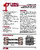



1. Overview
️· Function: The LTC1686 is a driver (transmitter) and the LTC1687 is a receiver (line receiver). They're designed to work together for data transmission over a single-wire line.
️· Key Features:
- Differential Signaling: Uses both A and B inputs for the receiver, providing noise immunity.
- Enable/Disable Functionality: Drivers can be enabled/disabled (DE). Receivers can be put into a high-impedance state (RE).
- Fault Detection: The LTC1687 has a fault condition, where an output current is forced if a fault is detected.
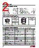
2. Pin Functions:
Let's condense the crucial pinouts:
️· LTC1686 (Driver):
- VDD: Positive supply (5V) – requires a 0.1µF bypass capacitor.
- D: Driver input – controls Y & Z outputs.
- GND: Ground
- Y: Non-inverting Driver Output.
- Z: Inverting Driver Output.
️· LTC1687 (Receiver):
- NC: No Connection (pins 1, 13).
- R: Receiver output.
- RE: Receiver Enable (low enables the receiver).
- D: Driver Input (for LTC1686 to control).
- GND: Ground
- Y: Noninverting Receiver Input.
- Z: Inverting Receiver Input.
- A: Non-inverting Receiver Input.
- B: Inverting Receiver Input.
- VDD: Positive supply (5V) – requires a 0.1µF bypass capacitor.
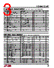
3. Truth Tables:
️· Transmitter Truth Table (LTC1686):
- When DE (Driver Enable) is high:
■ If D is high, Z is low and Y is high.
■ If D is low, Z is high and Y is low.
- When DE is low, the driver outputs are in a high-impedance state.
️· Receiver Truth Table (LTC1687):
- If A is greater than B by 300mV, R is high.
- If A is less than B by 300mV, R is low.
- If RE is high, the receiver output (R) is in a high-impedance state.
- If inputs A and B are shorted and voltages are between -7V and 12V, R will be high.
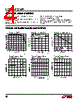
4. Test Circuits and Waveforms
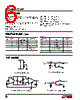
️· Driver DC Test Load (Figures 1 & 2): Shows how to test the driver's DC characteristics.
️· Driver/Receiver Timing Test Circuit (Figure 3): Demonstrates how to test the timing of the driver and receiver.
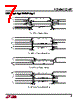
️· Driver Enable/Disable Timing (Figure 6): Shows waveforms for the enable and disable times for the driver.
️· Receiver Enable/Disable Timing (Figure 8): Shows the waveforms for the receiver enable/disable.
️· Propagation Delays (Figure 3 & 7): Provides waveforms to understand propagation delays.
Key Takeaways:
️· Differential Pair: The data transmission is a differential signal - it uses both A/B on the receiver and Y/Z on the driver. This provides better noise immunity.
️· Enable Control: The ability to enable/disable the driver/receiver is important for power saving and system control.
️· Standard Operating Conditions: The IC operates at 5V.
️· Fault Indication: The receiver offers a fault-detection mechanism for indicating error conditions.
1. Overview
️· Function: The LTC1686 is a driver (transmitter) and the LTC1687 is a receiver (line receiver). They're designed to work together for data transmission over a single-wire line.
️· Key Features:
- Differential Signaling: Uses both A and B inputs for the receiver, providing noise immunity.
- Enable/Disable Functionality: Drivers can be enabled/disabled (DE). Receivers can be put into a high-impedance state (RE).
- Fault Detection: The LTC1687 has a fault condition, where an output current is forced if a fault is detected.
2. Pin Functions:
Let's condense the crucial pinouts:
️· LTC1686 (Driver):
- VDD: Positive supply (5V) – requires a 0.1µF bypass capacitor.
- D: Driver input – controls Y & Z outputs.
- GND: Ground
- Y: Non-inverting Driver Output.
- Z: Inverting Driver Output.
️· LTC1687 (Receiver):
- NC: No Connection (pins 1, 13).
- R: Receiver output.
- RE: Receiver Enable (low enables the receiver).
- D: Driver Input (for LTC1686 to control).
- GND: Ground
- Y: Noninverting Receiver Input.
- Z: Inverting Receiver Input.
- A: Non-inverting Receiver Input.
- B: Inverting Receiver Input.
- VDD: Positive supply (5V) – requires a 0.1µF bypass capacitor.
3. Truth Tables:
️· Transmitter Truth Table (LTC1686):
- When DE (Driver Enable) is high:
■ If D is high, Z is low and Y is high.
■ If D is low, Z is high and Y is low.
- When DE is low, the driver outputs are in a high-impedance state.
️· Receiver Truth Table (LTC1687):
- If A is greater than B by 300mV, R is high.
- If A is less than B by 300mV, R is low.
- If RE is high, the receiver output (R) is in a high-impedance state.
- If inputs A and B are shorted and voltages are between -7V and 12V, R will be high.
4. Test Circuits and Waveforms
️· Driver DC Test Load (Figures 1 & 2): Shows how to test the driver's DC characteristics.
️· Driver/Receiver Timing Test Circuit (Figure 3): Demonstrates how to test the timing of the driver and receiver.
️· Driver Enable/Disable Timing (Figure 6): Shows waveforms for the enable and disable times for the driver.
️· Receiver Enable/Disable Timing (Figure 8): Shows the waveforms for the receiver enable/disable.
️· Propagation Delays (Figure 3 & 7): Provides waveforms to understand propagation delays.
Key Takeaways:
️· Differential Pair: The data transmission is a differential signal - it uses both A/B on the receiver and Y/Z on the driver. This provides better noise immunity.
️· Enable Control: The ability to enable/disable the driver/receiver is important for power saving and system control.
️· Standard Operating Conditions: The IC operates at 5V.
️· Fault Indication: The receiver offers a fault-detection mechanism for indicating error conditions.
| Part No. | LTC1686CS8 |
| Manufacturer | LINER |
| Size | 285 Kbytes |
| Pages | 12 pages |
| Description | 52Mbps Precision Delay RS485 Fail-Safe Transceivers |
| ¿ALLDATASHEET es útil para Ud.? [ DONATE ] |
Todo acerca de Alldatasheet | Publicidad | Contáctenos | Política de Privacidad | Enlace a la hoja de datos | Intercambio de Enlaces | Lista de Fabricantes All Rights Reserved©Alldatasheet.com |
| Russian : Alldatasheetru.com | Korean : Alldatasheet.co.kr | Spanish : Alldatasheet.es | French : Alldatasheet.fr | Italian : Alldatasheetit.com Portuguese : Alldatasheetpt.com | Polish : Alldatasheet.pl | Vietnamese : Alldatasheet.vn Indian : Alldatasheet.in | Mexican : Alldatasheet.com.mx | British : Alldatasheet.co.uk | New Zealand : Alldatasheet.co.nz |
|
Family Site : ic2ic.com |
icmetro.com |
 Mexican ▼
  English
 Chinese
 German
 Japanese
 Russian
 Korean
 Spanish
 French
 Italian
 Portuguese
 Polish
 Vietnamese
 Indian
 British
 New Zealand