 |
Motor de Búsqueda de Datasheet de Componentes Electrónicos |
|
|
Motor de Búsqueda de Datasheet de Componentes Electrónicos |
|
The question interval is too short.
Please try again in a few seconds.

Hello, Please ask a question about MP7610CS Datasheet
# Example questions:
➢ What happens to the analog outputs of the mp7610 when the rst (reset) signal is activated (set to low)?
➢ What can be done to improve the accuracy of the output voltage when driving remote devices with the mp7610?
➢ What is the primary purpose of the ld (load) signal in the mp7610's serial interface?
| Part No. | MP7610CS |
| Manufacturer | EXAR |
| Size | 571 Kbytes |
| Pages | 16 pages |
| Description | D/A Converter with Output Amplifier and Serial Data/Address mP Control Logic |


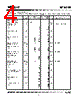
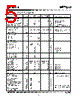







1. Overview: What is the MP7610?
️· Type: It's an 8-channel Digital-to-Analog Converter (DAC). This means it takes digital input data and converts it into analog voltage outputs.
️· Serial Interface: It uses a serial data interface (3-wire: LD, CLK, SDI) for communication. This interface minimizes the number of pins required, which is good for smaller circuit boards.
️· Reset Function: It includes a reset function (RST) that forces all DAC outputs to 0 volts.
️· Package/Application: Designed for compact applications, likely embedded systems or those requiring precise analog voltage control.
️· Industrial Temperature Range: Extended industrial temp range of -40°C to +85°C.
2. Serial Interface: How to Communicate with the MP7610
️· Signals:
- SDI (Serial Data In): This is where you send the digital data to be converted. Data is shifted in bit-by-bit.
- CLK (Clock): This signal synchronizes the shifting of data into the DAC.
- LD (Latch/Load): This signal has two critical functions:
■ When high, it enables data shifting into the internal shift register.
■ When brought low, it loads the data from the shift register into the DACs and also outputs the data. The output goes to a hi-z state.
️· Shifting Data: Data is shifted in serially, starting with the most significant bit (MSB).
️· Loading Data: When LD goes low, the data in the shift register is sent to the DACs, creating the analog output voltage.
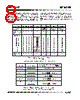
3. Truth Table (Digital Function Truth Table)
This table describes all possible operations and states of the MP7610. Key aspects are:
️· Data Shifting: To shift in data, LD must be high. Each clock pulse (CLK) shifts one bit into the internal register.
️· Loading Data: When LD is brought low, the data is loaded into the DACs, creating the analog output voltage, and the output data goes Hi-Z.
️· Reset: When RST is set to low, all DAC outputs are forced to 0V.
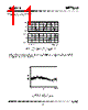
4. DAC Output (Ideal DAC Output vs. Input Code)
️· Output Voltage Formula: The ideal output voltage can be calculated using the formula: `Output Voltage = 10 * (-1 + 2 * D)`. (where D is the digital input value).
- `Vr = 5V` - this indicates the range of voltage that is expected to be produced by the system.
- `D = 16384` - This is the maximum digital input value for the 14-bit DAC section.
️· Important Note: The table provides *ideal* output values. In a real-world system, the accuracy will be affected by factors like component tolerances, power supply noise, and temperature variations. Refer to the "Electrical Characteristics" section for more details.
Summary Table
| Signal | Function |
|---|---|
| SDI | Serial Data In |
| CLK | Clock |
| LD | Load and Latch |
| RST | Reset |
| MSB | Most Significant Bit |
| D | Digital Input |
| Hi-Z | High Impedance (output disabled) |
| Vr | Voltage Reference |
1. Overview: What is the MP7610?
️· Type: It's an 8-channel Digital-to-Analog Converter (DAC). This means it takes digital input data and converts it into analog voltage outputs.
️· Serial Interface: It uses a serial data interface (3-wire: LD, CLK, SDI) for communication. This interface minimizes the number of pins required, which is good for smaller circuit boards.
️· Reset Function: It includes a reset function (RST) that forces all DAC outputs to 0 volts.
️· Package/Application: Designed for compact applications, likely embedded systems or those requiring precise analog voltage control.
️· Industrial Temperature Range: Extended industrial temp range of -40°C to +85°C.
2. Serial Interface: How to Communicate with the MP7610
️· Signals:
- SDI (Serial Data In): This is where you send the digital data to be converted. Data is shifted in bit-by-bit.
- CLK (Clock): This signal synchronizes the shifting of data into the DAC.
- LD (Latch/Load): This signal has two critical functions:
■ When high, it enables data shifting into the internal shift register.
■ When brought low, it loads the data from the shift register into the DACs and also outputs the data. The output goes to a hi-z state.
️· Shifting Data: Data is shifted in serially, starting with the most significant bit (MSB).
️· Loading Data: When LD goes low, the data in the shift register is sent to the DACs, creating the analog output voltage.
3. Truth Table (Digital Function Truth Table)
This table describes all possible operations and states of the MP7610. Key aspects are:
️· Data Shifting: To shift in data, LD must be high. Each clock pulse (CLK) shifts one bit into the internal register.
️· Loading Data: When LD is brought low, the data is loaded into the DACs, creating the analog output voltage, and the output data goes Hi-Z.
️· Reset: When RST is set to low, all DAC outputs are forced to 0V.
4. DAC Output (Ideal DAC Output vs. Input Code)
️· Output Voltage Formula: The ideal output voltage can be calculated using the formula: `Output Voltage = 10 * (-1 + 2 * D)`. (where D is the digital input value).
- `Vr = 5V` - this indicates the range of voltage that is expected to be produced by the system.
- `D = 16384` - This is the maximum digital input value for the 14-bit DAC section.
️· Important Note: The table provides *ideal* output values. In a real-world system, the accuracy will be affected by factors like component tolerances, power supply noise, and temperature variations. Refer to the "Electrical Characteristics" section for more details.
Summary Table
| Signal | Function |
|---|---|
| SDI | Serial Data In |
| CLK | Clock |
| LD | Load and Latch |
| RST | Reset |
| MSB | Most Significant Bit |
| D | Digital Input |
| Hi-Z | High Impedance (output disabled) |
| Vr | Voltage Reference |
| Part No. | MP7610CS |
| Manufacturer | EXAR |
| Size | 571 Kbytes |
| Pages | 16 pages |
| Description | D/A Converter with Output Amplifier and Serial Data/Address mP Control Logic |
| ¿ALLDATASHEET es útil para Ud.? [ DONATE ] |
Todo acerca de Alldatasheet | Publicidad | Contáctenos | Política de Privacidad | Enlace a la hoja de datos | Intercambio de Enlaces | Lista de Fabricantes All Rights Reserved©Alldatasheet.com |
| Russian : Alldatasheetru.com | Korean : Alldatasheet.co.kr | Spanish : Alldatasheet.es | French : Alldatasheet.fr | Italian : Alldatasheetit.com Portuguese : Alldatasheetpt.com | Polish : Alldatasheet.pl | Vietnamese : Alldatasheet.vn Indian : Alldatasheet.in | Mexican : Alldatasheet.com.mx | British : Alldatasheet.co.uk | New Zealand : Alldatasheet.co.nz |
|
Family Site : ic2ic.com |
icmetro.com |
 Mexican ▼
  English
 Chinese
 German
 Japanese
 Russian
 Korean
 Spanish
 French
 Italian
 Portuguese
 Polish
 Vietnamese
 Indian
 British
 New Zealand