|
Motor de Búsqueda de Datasheet de Componentes Electrónicos |
|
|
Motor de Búsqueda de Datasheet de Componentes Electrónicos |
|
LTM4650-1 Datasheet(PDF) 9 Page - Linear Technology |
|
|
|||||||||||||||||||||||||||||
LTM4650-1 Datasheet(HTML) 9 Page - Linear Technology |
|
|
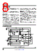
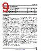
9 / 34 page  LTM4647 9 4647fb For more information www.linear.com/LTM4647 OPERATION Power Module Description The LTM4647 is a high performance single output stand- alone nonisolated switching mode DC/DC power supply. It can provide a 30A output with few external input and output capacitors. This module provides precisely regu- lated output voltages programmable via external resistors from 0.6V DC to 1.8V DC over a 4.7V to 15V input range. The typical application schematic is shown in Figure 23 and Figure 24. The LTM4647 has an integrated constant-frequency cur- rent mode regulator, power MOSFETs, inductor,and other supportingdiscretecomponents.Theswitchingfrequency range is optimized from 400kHz to 700kHz, depending on outputvoltage.Forswitchingnoise-sensitiveapplications, it can externally program to or be synchronized to a clock from 400kHz to 800kHz subject to minimum on-time and inductor ripple current limitations. See the Applications Information section. The LTM4647 is designed to use either external or internal controlloopcompensationbyshortingCOMPbandCOMPa pins together. With current mode control, the internal loop compensation has sufficient stability margins and good transient performance with a wide range of output capacitors, even with all ceramic output capacitors. Table 5 provides a guideline for input and output capacitances for several different output conditions using the internal loop compensation. The LTpowerCAD® design tool is available to download for optimizing the loop stability and transient response. Current mode control provides cycle-by-cycle fast current limit in an overcurrent condition. An internal overvoltage monitor protects the output voltage in the event of an overvoltage >10%. The top MOSFET is turned off and the bottom MOSFET is turned on until the output is cleared. Pulling the RUN pin below 1.35V forces the regulator into a shutdown state. The TRACK/SS pin is used for pro- gramming the output voltage ramp and voltage tracking during start-up. See the Application Information section. Multiphase operation can be easily employed by cascad- ing the MODE/PLLIN input to the CLKOUT output. See the ApplicationsInformationsectionandFigure25forexample. For high reliability environment, N+1 phase redundancy can be easily implemented in LTM4647 together with a hot swap controller, such as the LTC®4226, for extra system protection. By connecting the HIZB pin to the gate of the hot swap switch, any fault channel can be disconnected while the rest of the system is not affected. See Applica- tions Information section and Figure 27 for example. High efficiency at light loads can be accomplished with phase shedding in multiphase operation or with selectable pulse-skipping mode or Burst Mode operation in single phase operation. Efficiency graphs are provided for light load operation in the Typical Performance Characteristics section. Aremotesenseamplifierisprovidedforaccuratelysensing output voltages at the load point. A TEMP+ and TEMP– pins are provided to allow the internal device temperature to be monitored using an onboard diode connected PNP transistor. DECOUPLING REQUIREMENTS SYMBOL PARAMETER CONDITIONS MIN TYP MAX UNITS CIN External Input Capacitor Requirement (VIN = 4.7V to 15V, VOUT = 1V) IOUT = 30A 44 µF COUT External Output Capacitor Requirement (VIN = 4.7V to 15V, VOUT = 1V) IOUT = 30A 440 µF |
|
Enlace URL |
| ¿ALLDATASHEET es útil para Ud.? [ DONATE ] |
Todo acerca de Alldatasheet | Publicidad | Contáctenos | Política de Privacidad | Enlace a la hoja de datos | Intercambio de Enlaces | Lista de Fabricantes All Rights Reserved©Alldatasheet.com |
| Russian : Alldatasheetru.com | Korean : Alldatasheet.co.kr | Spanish : Alldatasheet.es | French : Alldatasheet.fr | Italian : Alldatasheetit.com Portuguese : Alldatasheetpt.com | Polish : Alldatasheet.pl | Vietnamese : Alldatasheet.vn Indian : Alldatasheet.in | Mexican : Alldatasheet.com.mx | British : Alldatasheet.co.uk | New Zealand : Alldatasheet.co.nz |
|
Family Site : ic2ic.com |
icmetro.com |
 Mexican ▼
 English
 Chinese
 German
 Japanese
 Russian
 Korean
 Spanish
 French
 Italian
 Portuguese
 Polish
 Vietnamese
 Indian
 Mexican
 British
 New Zealand