|
Motor de Búsqueda de Datasheet de Componentes Electrónicos |
|
|
Motor de Búsqueda de Datasheet de Componentes Electrónicos |
|
STM32H7B3II Datasheet(PDF) 122 Page - STMicroelectronics |
|
|
|||||||||||||||||||||||||||||
STM32H7B3II Datasheet(HTML) 122 Page - STMicroelectronics |
|
|
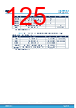
122 / 238 page  Speed Symbol Parameter conditions Min(1) Max(1) Unit 01 Fmax(2) Maximum frequency C=50 pF, 1.62 V≤VDD≤2.7 V - 50 MHz C=30 pF, 1.62 V≤VDD≤2.7 V - 58 C=10 pF, 1.62 V≤VDD≤2.7 V - 66 tr/tf(3) Output high to low level fall time and output low to high level rise time C=50 pF, 1.62 V≤VDD≤2.7 V - 6.6 ns C=30 pF, 1.62 V≤VDD≤2.7 V - 4.8 C=10 pF, 1.62 V≤VDD≤2.7 V - 3 10 Fmax(2) Maximum frequency C=50 pF, 1.62 V≤VDD≤2.7 V(4) - 55 MHz C=30 pF, 1.62 V≤VDD≤2.7 V(4) - 80 C=10 pF, 1.62 V≤VDD≤2.7 V(4) - 133 tr/tf(3) Output high to low level fall time and output low to high level rise time C=50 pF, 1.62 V≤VDD≤2.7 V(4) - 5.8 ns C=30 pF, 1.62 V≤VDD≤2.7 V(4) - 4 C=10 pF, 1.62 V≤VDD≤2.7 V(4) - 2.4 11 Fmax(2) Maximum frequency C=50 pF, 1.62 V≤VDD≤2.7 V(4) - 60 MHz C=30 pF, 1.62 V≤VDD≤2.7 V(4) - 90 C=10 pF, 1.62 V≤VDD≤2.7 V(4) - 175 tr/tf(3) Output high to low level fall time and output low to high level rise time C=50 pF, 1.62 V≤VDD≤2.7 V(4) - 5.3 ns C=30 pF, 1.62 V≤VDD≤2.7 V(4) - 3.6 C=10 pF, 1.62 V≤VDD≤2.7 V(4) - 1.9 1. Guaranteed by design. 2. The maximum frequency is defined with the following conditions: (tr+tf) ≤ 2/3 T, skew ≤ 1/20 T, 45%<Duty cycle<55% 3. The fall and rise times are defined between 90% and 10% and between 10% and 90% of the output waveform, respectively. 4. Compensation system enabled. Analog switch between ports Pxy_C and Pxy PA0_C, PA1_C, PC2_C and PC3_C can be connected internally to PA0, PA1, PC2 and PC3, respectively (refer to SYSCFG_PMCR register in RM0468 reference manual). The switch is controlled by VDDSWITCH voltage level. It is defined through BOOSTVDDSEL bit of SYSCFG_PMCR. If the switch is closed the switch characteristics are given in the table below. Table 70. Pxy_C and Pxy analog switch characteristics Parameter Conditions Min Typ Max Unit Switch impedance Switch control boosted - - 315 Ω Switch control not boosted VDDSWITCH > 2.7 V - - 315 VDDSWITCH > 2.4 V - - 335 VDDSWITCH > 2.0 V - - 390 VDDSWITCH > 1.8 V - - 445 VDDSWITCH > 1.62 V - - 550 6.3.17 NRST pin characteristics The NRST pin input driver uses CMOS technology. It is connected to a permanent pull-up resistor, RPU (see Table 65. I/O static characteristics). Unless otherwise specified, the parameters given in Table 71. NRST pin characteristics are derived from tests performed under the ambient temperature and VDD supply voltage conditions summarized in Table 22. General operating conditions. STM32H7B3xI Operating conditions DS13139 - Rev 8 page 122/238 |
|
Enlace URL |
| ¿ALLDATASHEET es útil para Ud.? [ DONATE ] |
Todo acerca de Alldatasheet | Publicidad | Contáctenos | Política de Privacidad | Enlace a la hoja de datos | Intercambio de Enlaces | Lista de Fabricantes All Rights Reserved©Alldatasheet.com |
| Russian : Alldatasheetru.com | Korean : Alldatasheet.co.kr | Spanish : Alldatasheet.es | French : Alldatasheet.fr | Italian : Alldatasheetit.com Portuguese : Alldatasheetpt.com | Polish : Alldatasheet.pl | Vietnamese : Alldatasheet.vn Indian : Alldatasheet.in | Mexican : Alldatasheet.com.mx | British : Alldatasheet.co.uk | New Zealand : Alldatasheet.co.nz |
|
Family Site : ic2ic.com |
icmetro.com |
 Mexican ▼
 English
 Chinese
 German
 Japanese
 Russian
 Korean
 Spanish
 French
 Italian
 Portuguese
 Polish
 Vietnamese
 Indian
 Mexican
 British
 New Zealand