 |
Motor de Búsqueda de Datasheet de Componentes Electrónicos |
|
|
Motor de Búsqueda de Datasheet de Componentes Electrónicos |
|
MASTERGAN1 Datasheet(PDF) 21 Page - STMicroelectronics |
|
|
|||||||||||||||||||||||||||||
MASTERGAN1 Datasheet(HTML) 21 Page - STMicroelectronics |
|
|
21 / 27 page 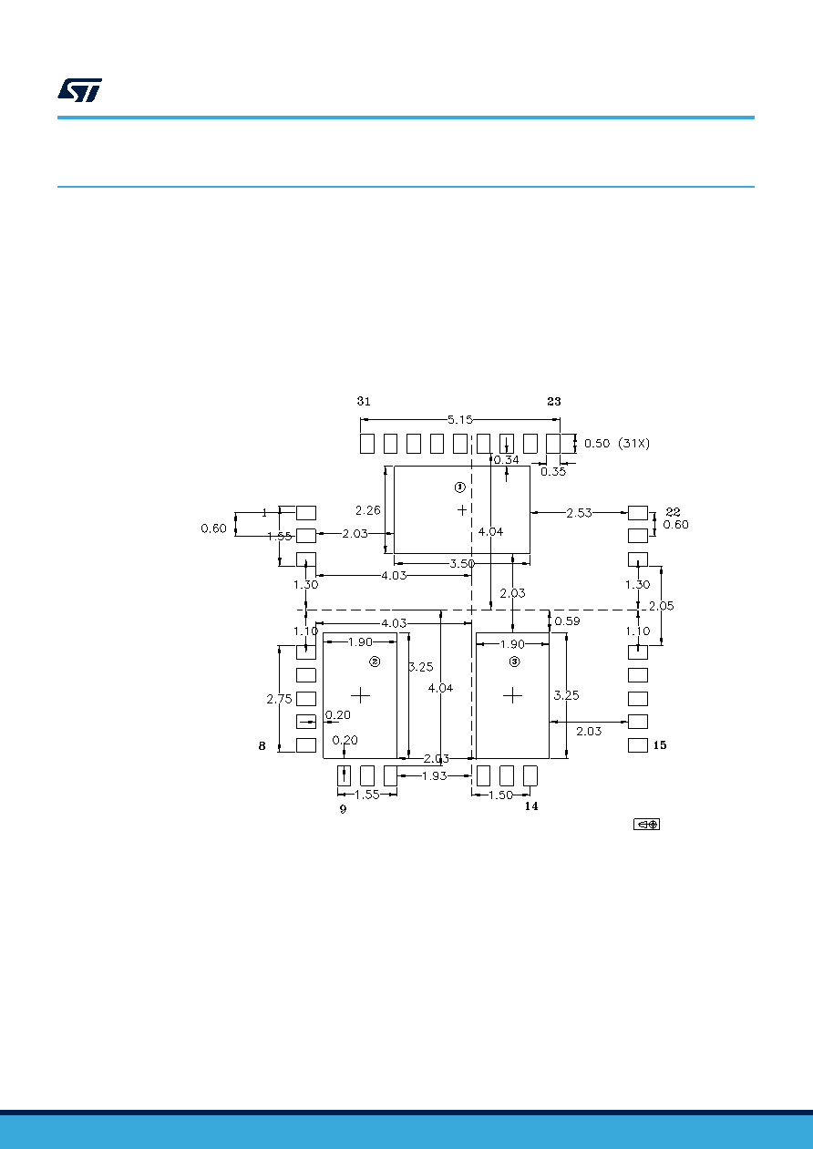 9 Suggested footprint The MASTERGAN1 footprint for the PCB layout is usually defined based on several design factors such as assembly plant technology capabilities and board component density. For easy device usage and evaluation, ST provides the following footprint design, which is suitable for the largest variety of PCBs. The following footprint indicates the copper area which should be free from the solder mask, while the copper area shall extend beyond the indicated areas especially for EP2 and EP3. To aid thermal dissipation, it is recommended to add thermal vias under these EPADs to transfer and dissipate device heat to the other PCB copper layers. A PCB layout example is available with the MASTERGAN1 evaluation board. Figure 22. Suggested footprint (top view drawing) TOP VIEW Dimensions in mm MASTERGAN1 Suggested footprint DS13417 - Rev 3 page 21/27 |
|
Enlace URL |
| ¿ALLDATASHEET es útil para Ud.? [ DONATE ] |
Todo acerca de Alldatasheet | Publicidad | Contáctenos | Política de Privacidad | Enlace a la hoja de datos | Intercambio de Enlaces | Lista de Fabricantes All Rights Reserved©Alldatasheet.com |
| Russian : Alldatasheetru.com | Korean : Alldatasheet.co.kr | Spanish : Alldatasheet.es | French : Alldatasheet.fr | Italian : Alldatasheetit.com Portuguese : Alldatasheetpt.com | Polish : Alldatasheet.pl | Vietnamese : Alldatasheet.vn Indian : Alldatasheet.in | Mexican : Alldatasheet.com.mx | British : Alldatasheet.co.uk | New Zealand : Alldatasheet.co.nz |
|
Family Site : ic2ic.com |
icmetro.com |
 Mexican ▼
 English
 Chinese
 German
 Japanese
 Russian
 Korean
 Spanish
 French
 Italian
 Portuguese
 Polish
 Vietnamese
 Indian
 Mexican
 British
 New Zealand


