|
Motor de Búsqueda de Datasheet de Componentes Electrónicos |
|
|
Motor de Búsqueda de Datasheet de Componentes Electrónicos |
|
DER-111 Datasheet(PDF) 6 Page - Power Integrations, Inc. |
|
|
|||||||||||||||||||||||||||||
DER-111 Datasheet(HTML) 6 Page - Power Integrations, Inc. |
|
|
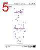
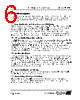
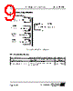
6 / 23 page  DER-111 3.15 W General Purpose Adapter October 26, 2005 Page 6 of 23 Power Integrations Tel: +1 408 414 9200 Fax: +1 408 414 9201 www.powerint.com 5 Circuit Description This circuit is configured as a Flyback operating in discontinuous conduction mode. The low standby consumption is achieved by using a high gain opto-coupler, using a bias winding that provides about 8 V during no-load, and by designing a low-capacitance transformer. 5.1 Input Rectification, Bulk Capacitance and EMI Filtering AC input power is rectified by a full bridge, consisting of D1 through D4. The rectified DC is then filtered by the bulk storage capacitors C1 and C2. Inductor L1 and Ferrite bead L2 separate C1 and C2 from each other. L1, C1 and C2 form a pi ( π) filter, which attenuates conducted differential-mode EMI noise. Fusible resistor RF1 has multiple functions. It is a fuse, an in-rush current limiting device, a final low pass filter stage (with C1) for conducted EMI attenuation and an initial stage of input surge voltage attenuation. 5.2 Primary DRAIN Voltage Clamp Circuit The DRAIN voltage clamp circuit is comprised of Zener diode VR1, R1 and diode D5. D5 and VR1 clamp the amplitude of the voltage spike that the transformer leakage inductance generates, at switch turn-off, to keep it beneath the device’s maximum DRAIN to SOURCE voltage rating (700 V). R1 damps the high frequency ringing caused by leakage inductance, which improves the conducted EMI performance of the circuit. The reflected output voltage VOR, which is determined by the transformer turns ratio (13:1), has been kept low (70 V) to minimize the power dissipation in the clamp circuit. 5.3 Auxiliary Bias Supply The auxiliary bias supply circuit is made up of the primary-side transformer bias winding, diode D6 and capacitor C5. D6 rectifies the output of the winding and C5 filters it. The winding was given just enough turns so that its minimum output voltage stays at 7V at no- load to minimize power consumption. C4 is the standard BP pin decoupling capacitor, which should always be a 50 V 0.1 µF ceramic capacitor that is located close to the IC. R3 and C9 are compensation network, along with the Linkswitch Control pin resistance, form a pole and a zero to stabilize the control loop. 5.4 Output Rectification and Filtering Output rectification and filtering are accomplished by Schottky diode D7, capacitors C6 and C7. D7 rectifies the output of the transformer, T1. 5.5 Output Voltage Sensing and Feedback Resistors R4, Zener diode VR2 and opto-isolator U2 sense the output voltage and feedback to the LinkSwitch. C10 provides power for the LinkSwitch during the time of power up, it also acts as a soft start capacitor. |
|
|
Enlace URL |
| ¿ALLDATASHEET es útil para Ud.? [ DONATE ] |
Todo acerca de Alldatasheet | Publicidad | Contáctenos | Política de Privacidad | Enlace a la hoja de datos | Intercambio de Enlaces | Lista de Fabricantes All Rights Reserved©Alldatasheet.com |
| Russian : Alldatasheetru.com | Korean : Alldatasheet.co.kr | Spanish : Alldatasheet.es | French : Alldatasheet.fr | Italian : Alldatasheetit.com Portuguese : Alldatasheetpt.com | Polish : Alldatasheet.pl | Vietnamese : Alldatasheet.vn Indian : Alldatasheet.in | Mexican : Alldatasheet.com.mx | British : Alldatasheet.co.uk | New Zealand : Alldatasheet.co.nz |
|
Family Site : ic2ic.com |
icmetro.com |
 Mexican ▼
 English
 Chinese
 German
 Japanese
 Russian
 Korean
 Spanish
 French
 Italian
 Portuguese
 Polish
 Vietnamese
 Indian
 Mexican
 British
 New Zealand