|
Motor de Búsqueda de Datasheet de Componentes Electrónicos |
|
|
Motor de Búsqueda de Datasheet de Componentes Electrónicos |
|
CS902-A-R Datasheet(PDF) 3 Page - Richtek Technology Corporation |
|
|
|||||||||||||||||||||||||||||
CS902-A-R Datasheet(HTML) 3 Page - Richtek Technology Corporation |
|
|
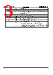
3 / 15 page 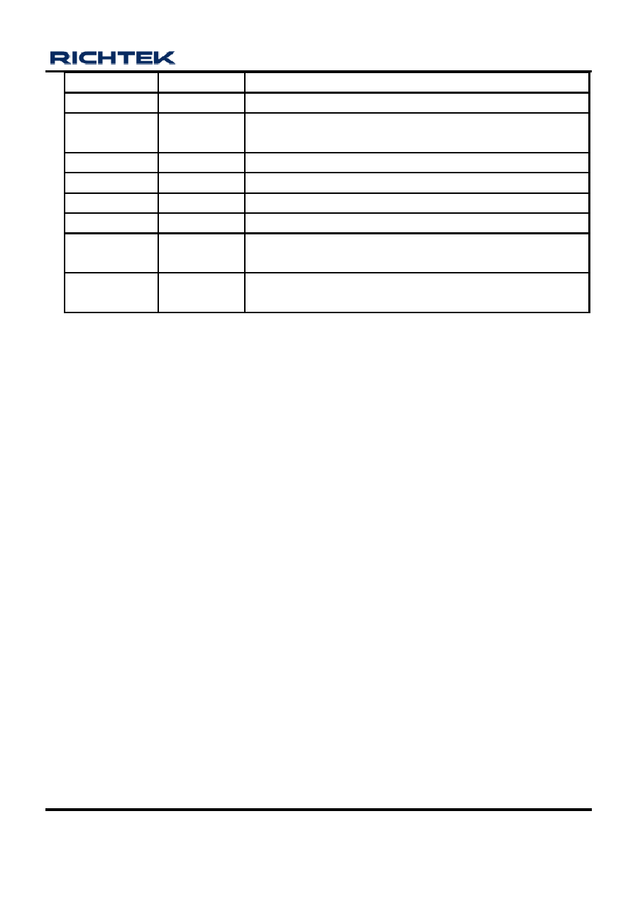 Conceptual CS902-A-R www.richtek.com June 13, 2013 3 32 VSUP VDD of OPAMP. 33 EN Chip enable 34 VGH Output sensing pin for the VGH positive charge pump and power input voltage pin for the GPM. 35 VGHM Switch output for gate shaping function. 36 RE Discharge pin for gate shaping function. 37 OUTB1 Output sensing pin of the VI/O buck converter. 38,39 LXB1 Switch pins of the VI/O buck converter. 40 BOOT1 N-channel MOSFET gate drive voltage for the VI/O buck converter. Connect a capacitor from the switch node LXB1 to this pin. 41 Exposed Pad The Exposed Pad should be soldered to a large PCB and connected to PGND for maximum thermal dissipation. |
|
|
Enlace URL |
| ¿ALLDATASHEET es útil para Ud.? [ DONATE ] |
Todo acerca de Alldatasheet | Publicidad | Contáctenos | Política de Privacidad | Enlace a la hoja de datos | Intercambio de Enlaces | Lista de Fabricantes All Rights Reserved©Alldatasheet.com |
| Russian : Alldatasheetru.com | Korean : Alldatasheet.co.kr | Spanish : Alldatasheet.es | French : Alldatasheet.fr | Italian : Alldatasheetit.com Portuguese : Alldatasheetpt.com | Polish : Alldatasheet.pl | Vietnamese : Alldatasheet.vn Indian : Alldatasheet.in | Mexican : Alldatasheet.com.mx | British : Alldatasheet.co.uk | New Zealand : Alldatasheet.co.nz |
|
Family Site : ic2ic.com |
icmetro.com |
 Mexican ▼
 English
 Chinese
 German
 Japanese
 Russian
 Korean
 Spanish
 French
 Italian
 Portuguese
 Polish
 Vietnamese
 Indian
 Mexican
 British
 New Zealand