|
Motor de Búsqueda de Datasheet de Componentes Electrónicos |
|
|
Motor de Búsqueda de Datasheet de Componentes Electrónicos |
|
ADRF5420BCDZ-R7 Datasheet(PDF) 13 Page - Analog Devices |
|
|
|||||||||||||||||||||||||||||
ADRF5420BCDZ-R7 Datasheet(HTML) 13 Page - Analog Devices |
|
|
13 / 14 page 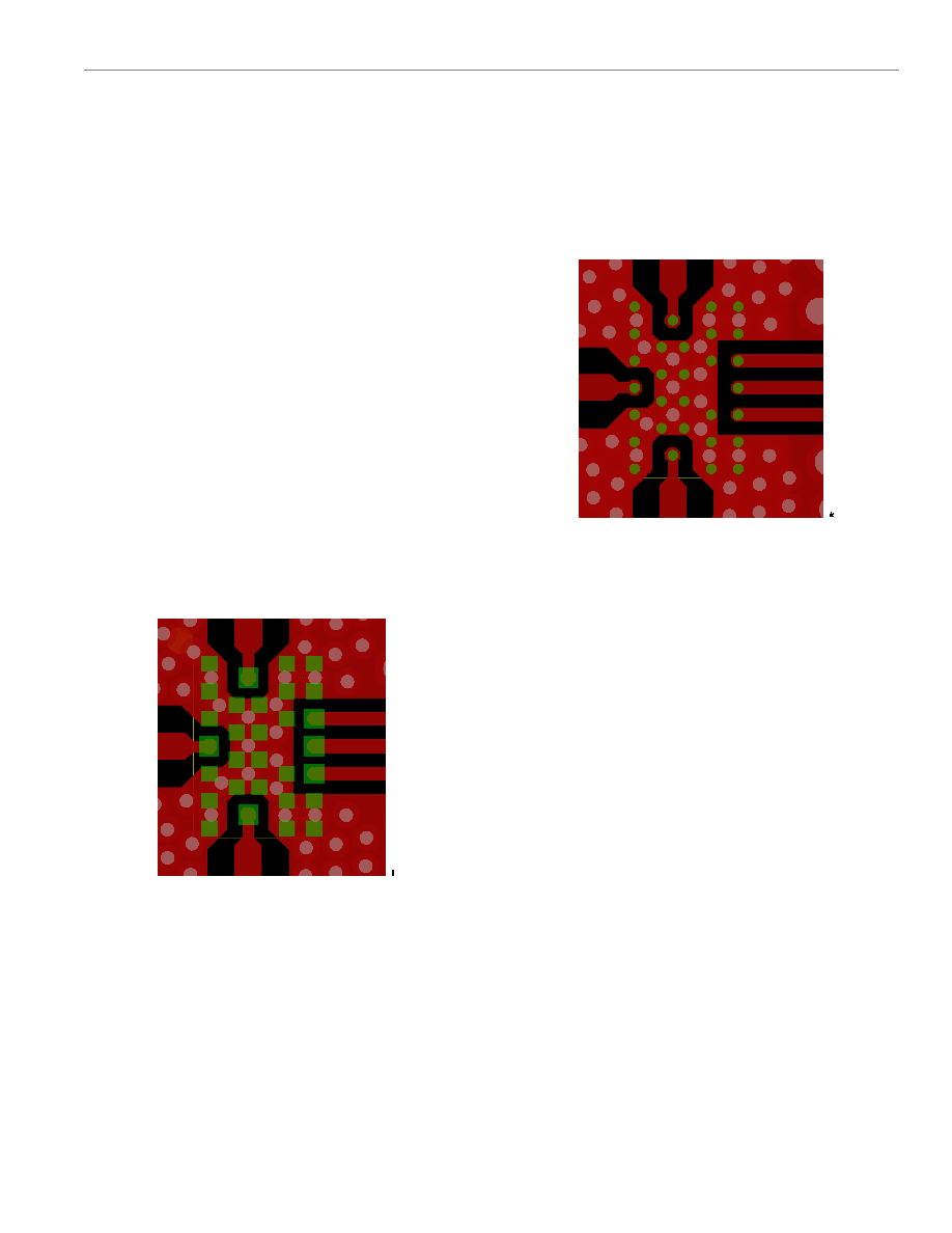 Data Sheet ADRF5420 APPLICATIONS INFORMATION analog.com Rev. 0 | 13 of 14 DIE ASSEMBLY The ADRF5420 complies with the standard RoHS reflow assembly process and can be assembled together with other surface-mount- ed technology (SMT) components in the same reflow cycle. The PCB must incorporate fiduicials close to the device to get the best pick and place accuracy. The top copper layer of the PCB is designed for optimum RF performance, and the solder mask and paste mask layers are designed for optimum assembly yield. The ground pads are drawn as solder mask defined. The signal pads are drawn as pad defined. The same solder mask and paste mask design is used for both pads. Alternatively, the ADRF5420 can be assembled without ap- plying a solder paste on the PCB. If no solder paste is applied, the device must be dipped into flux prior to placement on the PCB. Reflow Assembly with Solder Paste Solder mask openings of 175µm in a square shape are recom- mended for the signal and RF pads, and solder mask openings of 150µm in a square shape are recommended for the GND pads. Solder mask thickness must not exceed 50µm. Paste mask is drawn circular with a 150µm diameter. Using a stencil with 2mil thickness and no aperture reduction yields the optimum paste mask print. The device does not need any flux dipping during the pick and place process. Figure 20. Recommended Footprint for Solder Paste Reflow Assembly with Flux Dipping Solder mask openings in a circular shape and 130µm in diameter are recommended. Solder mask thickness must not exceed 50µm. Solder paste is not applied. The device is dipped into flux prior to placement on the board. Figure 21. Recommended Footprint for Flux Dip Assembly Assembly Durability The device is a bumped die. The bump composition is copper (Cu) pillar with a plated tin (Sn) and silver (Ag) solder-cap, which forms the device interconnect to PCB when it is attached with reflow. The integrity of the interconnect structures and solder joints are compro- mised by the accumulated stress over temperature due to a mis- match of the thermomechanical properties of the different materials in the complete assembly of the user hardware. The ADRF5420 fulfills the JEDEC JED47L requirements under the JESD22-A104 Condition J (0-100C) for 2300 temperature cycles while mounted on a 0.75mm thick laminate PCB, which is assembled using solder paste reflow and without any underfill material applied. Users must qualify their hardware for the environmental conditions aligned with their end-use requirements because differences in PCB properties and design, varied number of temperature cycles, soak and dwell times, and changes in temperature range, can affect thermome- chanical results. Note that using a proper underfill adhesive signifi- cantly improves the integrity of the device assembly by reducing the stress exposed to the interconnect structures and solder joints. |
|
|
Enlace URL |
| ¿ALLDATASHEET es útil para Ud.? [ DONATE ] |
Todo acerca de Alldatasheet | Publicidad | Contáctenos | Política de Privacidad | Enlace a la hoja de datos | Intercambio de Enlaces | Lista de Fabricantes All Rights Reserved©Alldatasheet.com |
| Russian : Alldatasheetru.com | Korean : Alldatasheet.co.kr | Spanish : Alldatasheet.es | French : Alldatasheet.fr | Italian : Alldatasheetit.com Portuguese : Alldatasheetpt.com | Polish : Alldatasheet.pl | Vietnamese : Alldatasheet.vn Indian : Alldatasheet.in | Mexican : Alldatasheet.com.mx | British : Alldatasheet.co.uk | New Zealand : Alldatasheet.co.nz |
|
Family Site : ic2ic.com |
icmetro.com |
 Mexican ▼
 English
 Chinese
 German
 Japanese
 Russian
 Korean
 Spanish
 French
 Italian
 Portuguese
 Polish
 Vietnamese
 Indian
 Mexican
 British
 New Zealand