|
Motor de Búsqueda de Datasheet de Componentes Electrónicos |
|
|
Motor de Búsqueda de Datasheet de Componentes Electrónicos |
|
SPT5400 Datasheet(PDF) 8 Page - Cadeka Microcircuits LLC. |
|
|
|||||||||||||||||||||||||||||
SPT5400 Datasheet(HTML) 8 Page - Cadeka Microcircuits LLC. |
|
|
8 / 8 page 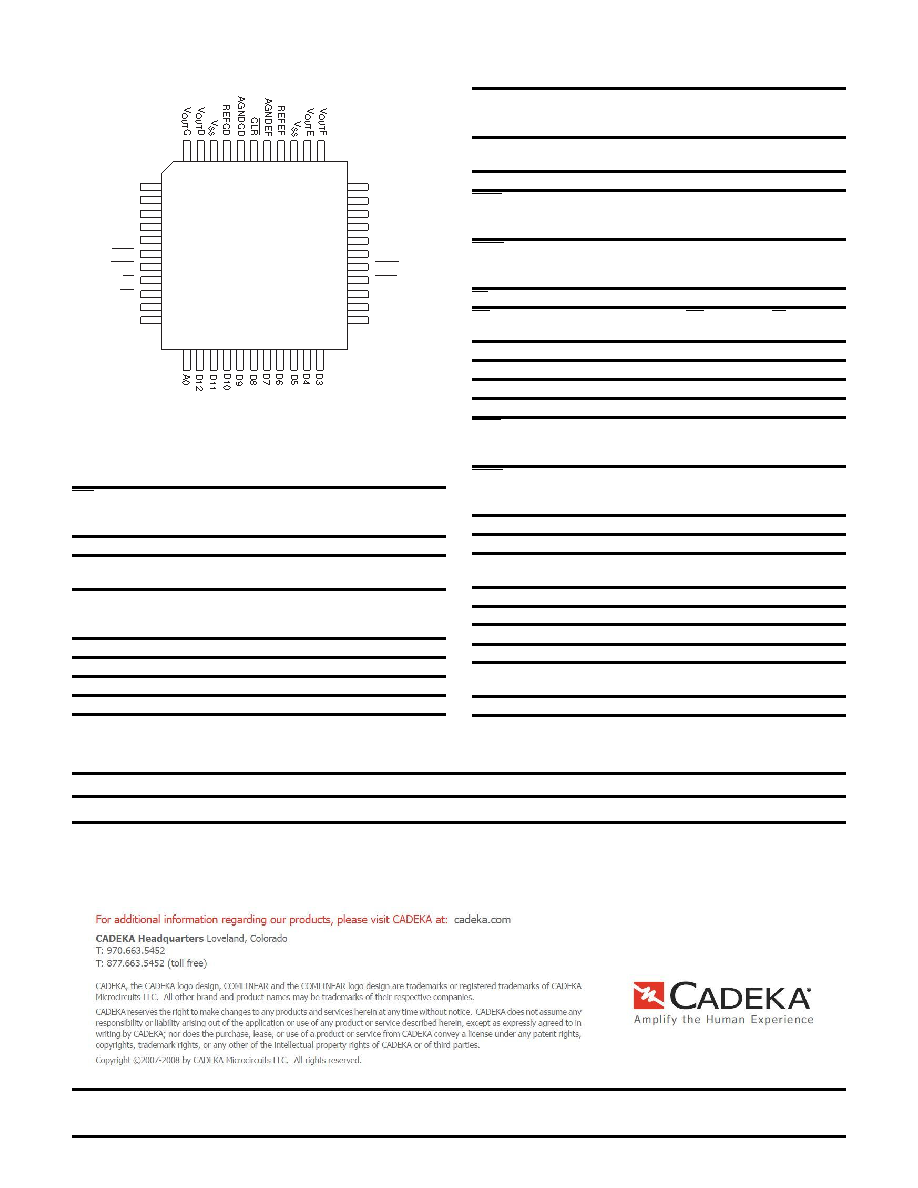 8 5/15/00 SPT5400 ORDERING INFORMATION PART NUMBER TEMPERATURE RANGE PACKAGE SPT5400SCP 0 to +70 °C 44L PLCC PIN ASSIGNMENTS Top View 44 1 VOUTB VOUTA VDD REFAB AGNDAB LDAB LDCD CS WR A2 A1 VOUTG VOUTH VDD REFGH AGNDGH GND LDGH LDEF D0 D1 D2 6 7 17 18 28 29 39 40 PIN FUNCTIONS Name Function CLR Clear input (active low). Driving this asynchronous input low sets the content of all latches to 1000hex. All DAC outputs are reset to AGNDxx. AGNDCD Analog ground for DAC C and DAC D. REFCD Reference voltage input for DAC C and DAC C. Bypass to AGNDCD with a 0.1 to 1 µF capacitor. VSS Negative power supply, –5 V (two pins). Connect both pins to the supply voltage. Bypass each pin to the system analog ground with a 0.1 µF capacitor. VOUTD DAC D output voltage. VOUTC DAC C output voltage. VOUTB DAC B output voltage. VOUTA DAC A output voltage. VDD Positive power supply, +5 V (two pins). Connect both pins to the supply voltage. Bypass each pin to the system analog ground with a 0.1 µF capacitor. REFAB Reference voltage input for DAC A and DAC B. Bypass to AGNDAB with a 0.1 to 1 µF capacitor. AGNDAB Analog ground for DAC A and DAC B. LDAB Load input (active low). Driving this asynchronous input low transfers the contents of the input latches A and B to the respective DAC latches. LDCD Load input (active low). Driving this asynchronous input low transfers the contents of the input latches C and D to the respective DAC latches. CS Chip select (active low). WR Write input (active low). WR along with CS load data into the DAC input latch selected by A0–A2. A2 Address bit 2. A1 Address bit 1. A0 Address bit 0. D12–D0 Data bits 12–0. (D0 = LSB) LDEF Load input (active low). Driving this asynchronous input low transfers the contents of the input latches E and F to the respective DAC latches. LDGH Load input (active low). Driving this asynchronous input low transfers the contents of the input latches G and H to the respective DAC latches. GND Digital ground. AGNDGH Analog ground for DAC G and DAC H. REFGH Reference voltage input for DAC G and DAC H. Bypass to AGNDGH with a 0.1 to 1 µF capacitor. VOUTH DAC H output voltage. VOUTG DAC G output voltage. VOUTF DAC F output voltage. VOUTE DAC E output voltage. REFEF Reference voltage input for DAC E and DAC F. Bypass to AGNDEF with a 0.1 to 1 µF capacitor. AGNDEF Analog ground for DAC E and DAC F. Name Function |
|
|
Enlace URL |
| ¿ALLDATASHEET es útil para Ud.? [ DONATE ] |
Todo acerca de Alldatasheet | Publicidad | Contáctenos | Política de Privacidad | Enlace a la hoja de datos | Intercambio de Enlaces | Lista de Fabricantes All Rights Reserved©Alldatasheet.com |
| Russian : Alldatasheetru.com | Korean : Alldatasheet.co.kr | Spanish : Alldatasheet.es | French : Alldatasheet.fr | Italian : Alldatasheetit.com Portuguese : Alldatasheetpt.com | Polish : Alldatasheet.pl | Vietnamese : Alldatasheet.vn Indian : Alldatasheet.in | Mexican : Alldatasheet.com.mx | British : Alldatasheet.co.uk | New Zealand : Alldatasheet.co.nz |
|
Family Site : ic2ic.com |
icmetro.com |
 Mexican ▼
 English
 Chinese
 German
 Japanese
 Russian
 Korean
 Spanish
 French
 Italian
 Portuguese
 Polish
 Vietnamese
 Indian
 Mexican
 British
 New Zealand