 |
Motor de Búsqueda de Datasheet de Componentes Electrónicos |
|
|
Motor de Búsqueda de Datasheet de Componentes Electrónicos |
|
ADP1613ARMZ-R7 Datasheet(PDF) 4 Page - Analog Devices |
|
|
|||||||||||||||||||||||||||||
ADP1613ARMZ-R7 Datasheet(HTML) 4 Page - Analog Devices |
|
|
4 / 28 page 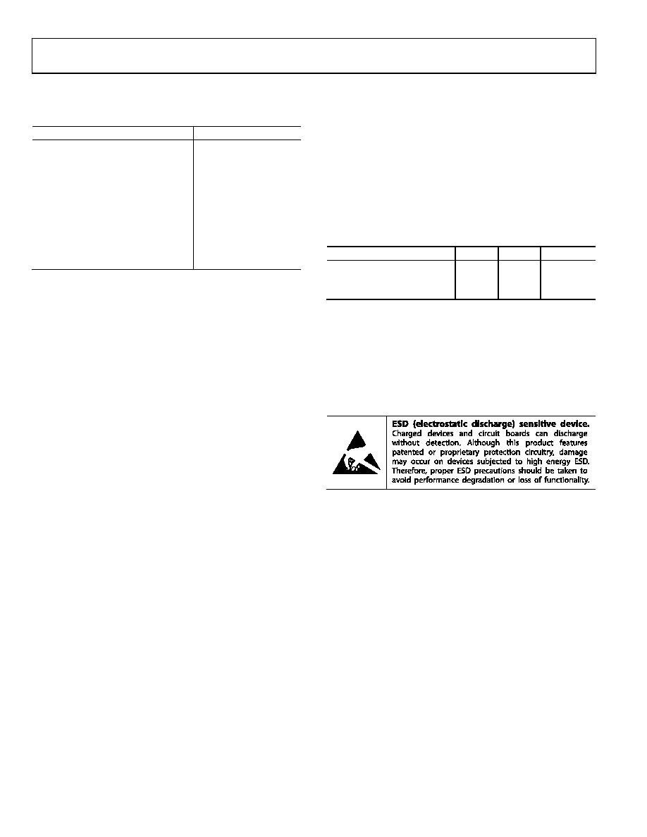 ADP1612/ADP1613 Rev. A | Page 4 of 28 ABSOLUTE MAXIMUM RATINGS Table 2. Parameter Rating VIN, EN, FB to GND −0.3 V to +6 V FREQ to GND −0.3 V to VIN + 0.3 V COMP to GND 1.0 V to 1.6 V SS to GND −0.3 V to +1.3 V SW to GND 21 V Operating Junction Temperature Range −40°C to +125°C Storage Temperature Range −65°C to +150°C Soldering Conditions JEDEC J-STD-020 ESD (Electrostatic Discharge) Human Body Model ±5 kV Stresses above those listed under Absolute Maximum Ratings may cause permanent damage to the device. This is a stress rating only; functional operation of the device at these or any other conditions above those indicated in the operational section of this specification is not implied. Exposure to absolute maximum rating conditions for extended periods may affect device reliability. Absolute maximum ratings apply individually only, not in combination. THERMAL RESISTANCE Junction-to-ambient thermal resistance (θJA) of the package is specified for the worst-case conditions, that is, a device soldered in a circuit board for surface-mount packages. The junction-to- ambient thermal resistance is highly dependent on the application and board layout. In applications where high maximum power dissipation exists, attention to thermal board design is required. The value of θJA may vary, depending on PCB material, layout, and environmental conditions. Table 3. Package Type θJA θJC Unit 8-Lead MSOP 2-Layer Board1 206.9 44.22 °C/W 4-Layer Board1 162.2 44.22 °C/W 1 Thermal numbers per JEDEC standard JESD 51-7. BOUNDARY CONDITION Modeled under natural convection cooling at 25°C ambient temperature, JESD 51-7, and 1 W power input with 2- and 4-layer boards. ESD CAUTION |
|
Enlace URL |
| ¿ALLDATASHEET es útil para Ud.? [ DONATE ] |
Todo acerca de Alldatasheet | Publicidad | Contáctenos | Política de Privacidad | Enlace a la hoja de datos | Intercambio de Enlaces | Lista de Fabricantes All Rights Reserved©Alldatasheet.com |
| Russian : Alldatasheetru.com | Korean : Alldatasheet.co.kr | Spanish : Alldatasheet.es | French : Alldatasheet.fr | Italian : Alldatasheetit.com Portuguese : Alldatasheetpt.com | Polish : Alldatasheet.pl | Vietnamese : Alldatasheet.vn Indian : Alldatasheet.in | Mexican : Alldatasheet.com.mx | British : Alldatasheet.co.uk | New Zealand : Alldatasheet.co.nz |
|
Family Site : ic2ic.com |
icmetro.com |
 Mexican ▼
 English
 Chinese
 German
 Japanese
 Russian
 Korean
 Spanish
 French
 Italian
 Portuguese
 Polish
 Vietnamese
 Indian
 Mexican
 British
 New Zealand


