 |
Motor de Búsqueda de Datasheet de Componentes Electrónicos |
|
|
Motor de Búsqueda de Datasheet de Componentes Electrónicos |
|
ADA4895-2ARMZ-R7 Datasheet(PDF) 21 Page - Analog Devices |
|
|
|||||||||||||||||||||||||||||
ADA4895-2ARMZ-R7 Datasheet(HTML) 21 Page - Analog Devices |
|
|
21 / 24 page 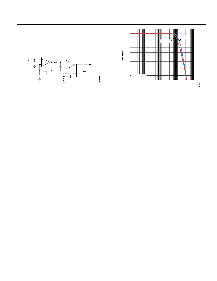 Data Sheet ADA4895-2 Rev. 0 | Page 21 of 24 HIGH GAIN BANDWIDTH APPLICATION The circuit in Figure 45 shows cascaded dual amplifier stages using the ADA4895-2. Each stage has a gain of +10 (+20 dB), making the output 100 times (+40 dB) the input. The total gain bandwidth product is approximately 9 GHz with the part operating on 6 mA of quiescent current (3 mA per amplifier). VOUT VIN RT 50 Ω RL 1k Ω RF 226 Ω CF 2pF C1 5pF RG 25.5 Ω RF 226 Ω CF 2pF RG 25.5 Ω R1 249 Ω Figure 45. Cascaded Amplifier Stages for High Gain Applications (G = +100) Figure 46 shows the large signal frequency response for two cases. The first case is with installed feedback capacitors (CF = 2 pF), and the second case is without these capacitors. Removing the 2 pF feedback capacitors from this circuit increases the bandwidth, but adds about 0.5 dB of peaking. 0 4 8 12 16 20 24 28 32 36 40 44 0.1 1 10 100 1000 FREQUENCY (MHz) CF = 2pF NO CF VOUT = 2V p-p G = +100 Figure 46. Large Signal Frequency Response, G = +100, VS = ±5 V To better balance the second stage and remove the current offset contribution, an R1C1 circuit can be sized to correct for any mis- match between the source impedance and the feedback network impedance on the input amplifier. (In the example shown in Figure 45, R1 = 249 Ω and C1 = 5 pF.) The offset of each amplifier is within the same statistical range. As configured, the offset of the output amplifier is not statistically significant to the overall offset of the system. Figure 46 was captured using a ±5 V supply; however, this circuit will also operate with supplies from ±1.5 V to ±5 V as long as the input and output headroom values are not violated. |
|
|
Enlace URL |
| ¿ALLDATASHEET es útil para Ud.? [ DONATE ] |
Todo acerca de Alldatasheet | Publicidad | Contáctenos | Política de Privacidad | Enlace a la hoja de datos | Intercambio de Enlaces | Lista de Fabricantes All Rights Reserved©Alldatasheet.com |
| Russian : Alldatasheetru.com | Korean : Alldatasheet.co.kr | Spanish : Alldatasheet.es | French : Alldatasheet.fr | Italian : Alldatasheetit.com Portuguese : Alldatasheetpt.com | Polish : Alldatasheet.pl | Vietnamese : Alldatasheet.vn Indian : Alldatasheet.in | Mexican : Alldatasheet.com.mx | British : Alldatasheet.co.uk | New Zealand : Alldatasheet.co.nz |
|
Family Site : ic2ic.com |
icmetro.com |
 Mexican ▼
 English
 Chinese
 German
 Japanese
 Russian
 Korean
 Spanish
 French
 Italian
 Portuguese
 Polish
 Vietnamese
 Indian
 Mexican
 British
 New Zealand


