|
Motor de Búsqueda de Datasheet de Componentes Electrónicos |
|
|
Motor de Búsqueda de Datasheet de Componentes Electrónicos |
|
LTC1098AC Datasheet(PDF) 14 Page - Linear Technology |
|
|
|||||||||||||||||||||||||||||
LTC1098AC Datasheet(HTML) 14 Page - Linear Technology |
|
|
14 / 28 page 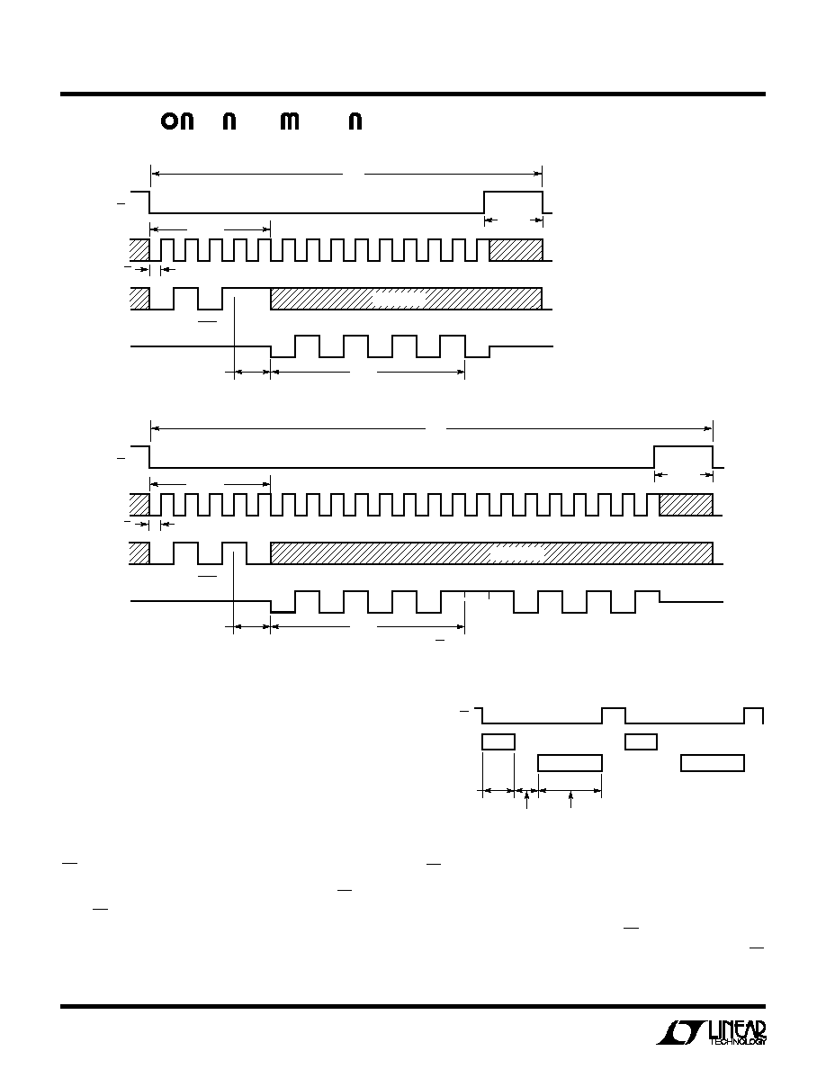 14 LTC1096/LTC1096L LTC1098/LTC1098L Data Transfer The CLK synchronizes the data transfer with each bit being transmitted on the falling CLK edge and captured on the rising CLK edge in both transmitting and receiving sys- tems. The LTC1098(L) first receives input data and then transmits back the A/D conversion result (half duplex). Because of the half duplex operation, DIN and DOUT may be tied together allowing transmission over just three wires: CS, CLK and DATA (DIN/DOUT). Data transfer is initiated by a falling chip select (CS) signal. After CS falls the LTC1098(L) looks for a start bit. After the start bit is received, the 3-bit input word is shifted into the DIN input which configures the LTC1098(L) and starts the conversion. After one null bit, the result of the conversion S APPLICATI I FOR ATIO CLK CS tCYC POWER DOWN tsuCS tWAKEUP DIN SGL/ DIFF MSBF B0* B1 B2 B3 B4 B5 B6 B7 NULL BIT Hi-Z DOUT tCONV tSMPL HI-Z START ODD/ SIGN DON'T CARE MSB-FIRST DATA (MSBF = 0) MSB-FIRST DATA (MSBF = 1) LTC1096/98 F02 CLK CS tCYC POWER DOWN tsuCS tWAKEUP DIN SGL/ DIFF MSBF B0 B1 B2 B3 B4 B5 B6 B7 NULL BIT Hi-Z DOUT tCONV tSMPL HI-Z START ODD/ SIGN DON'T CARE B7* B6 B5 B4 B3 B2 B1 *AFTER COMPLETING THE DATA TRANSFER, IF FURTHER CLOCKS ARE APPLIED WITH CS LOW, THE ADC WILL OUTPUT ZEROS INDEFINITELY. (MSB) (MSB) Figure 2. LTC1098(L) Operating Sequence Example: Differential Inputs (CH +, CH–) DIN 1 DIN 2 DOUT 1 DOUT 2 CS SHIFT MUX ADDRESS IN 1 NULL BIT SHIFT A/D CONVERSION RESULT OUT LTC1096/98 • AI01 is output on the DOUT line. At the end of the data exchange CS should be brought high. This resets the LTC1098(L) in preparation for the next data exchange. The LTC1096(L) does not require a configuration input word and has no DIN pin. A falling CS initiates data transfer as shown in the LTC1096(L) operating sequence. After CS falls, the first CLK pulse enables DOUT. After one null bit, |
|
Enlace URL |
| ¿ALLDATASHEET es útil para Ud.? [ DONATE ] |
Todo acerca de Alldatasheet | Publicidad | Contáctenos | Política de Privacidad | Enlace a la hoja de datos | Intercambio de Enlaces | Lista de Fabricantes All Rights Reserved©Alldatasheet.com |
| Russian : Alldatasheetru.com | Korean : Alldatasheet.co.kr | Spanish : Alldatasheet.es | French : Alldatasheet.fr | Italian : Alldatasheetit.com Portuguese : Alldatasheetpt.com | Polish : Alldatasheet.pl | Vietnamese : Alldatasheet.vn Indian : Alldatasheet.in | Mexican : Alldatasheet.com.mx | British : Alldatasheet.co.uk | New Zealand : Alldatasheet.co.nz |
|
Family Site : ic2ic.com |
icmetro.com |
 Mexican ▼
 English
 Chinese
 German
 Japanese
 Russian
 Korean
 Spanish
 French
 Italian
 Portuguese
 Polish
 Vietnamese
 Indian
 Mexican
 British
 New Zealand