|
Motor de Búsqueda de Datasheet de Componentes Electrónicos |
|
|
Motor de Búsqueda de Datasheet de Componentes Electrónicos |
|
ATF331M4 Datasheet(PDF) 13 Page - Agilent(Hewlett-Packard) |
|
|
|||||||||||||||||||||||||||||
ATF331M4 Datasheet(HTML) 13 Page - Agilent(Hewlett-Packard) |
|
|
13 / 17 page 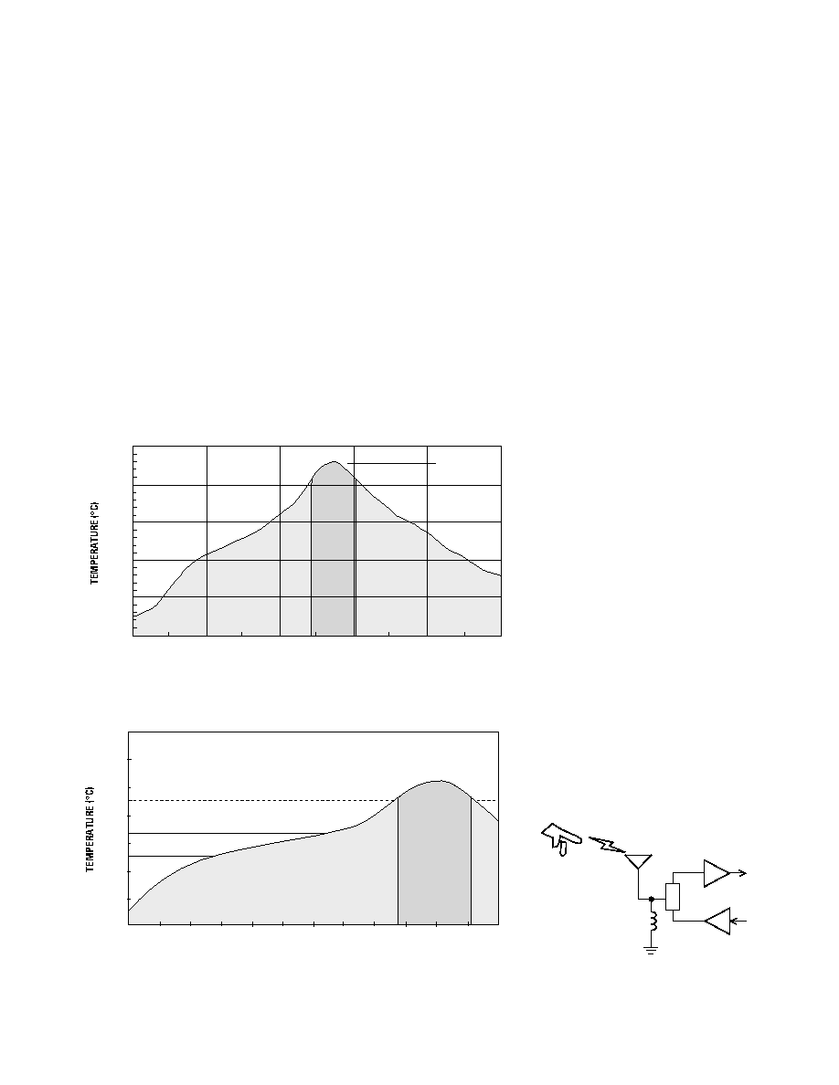 12 TIME (seconds) T MAX 0 0 50 100 150 200 250 60 Preheat Zone Cool Down Zone Reflow Zone 120 180 240 300 Figure 25. Lead-free Solder Reflow Profile. Figure 24. Leaded Solder Reflow Profile. TIME (seconds) Peak Temperature Min. 240 °C Max. 255 °C 0 0 50 150 100 221 200 250 300 350 60 90 30 120 150 210 180 270 300 330 240 360 Preheat 130 – 170 °C Min. 60s Max. 150s Reflow Time Min. 60s Max. 90s evaporating solvents from the solder paste. The reflow zone briefly elevates the temperature sufficiently to produce a reflow of the solder. The rates of change of tempera- ture for the ramp-up and cool- down zones are chosen to be low enough to not cause deformation of board or damage to compo- nents due to thermal shock. The maximum temperature in the reflow zone (Tmax) should not exceed 235 °C for leaded solder. These parameters are typical for a surface mount assembly process for the ATF-331M4. As a general guideline, the circuit board and components should only be exposed to the minimum temperatures and times the necessary to achieve a uniform reflow of solder. The recommended lead-free reflow profile is shown in Figure 25. Electrostatic Sensitivity FETs and RFICs are electrostatic discharge (ESD) sensitive de- vices. Agilent devices are manu- factured using a very robust and reliable PHEMT process, however, permanent damage may occur to these devices if they are sub- jected to high-energy electrostatic discharges. Electrostatic charges as high as several thousand volts (which readily accumulate on the human body and on test equip- ment) can discharge without detection and may result in failure or degradation in perfor- mance and reliability. Electronic devices may be subjected to ESD damage in any of the following areas: • Storage & handling • Inspection • Assembly & testing • In-circuit use The ATF-331M4 is an ESD Class 1 device. Therefore, proper ESD precautions are recom- mended when handling, inspect- ing, testing, and assembling these devices to avoid damage. Any user-accessible points in wireless equipment (e.g. antenna or battery terminals) provide an opportunity for ESD damage. For circuit applications in which the ATF-331M4 is used as an input or output stage with close coupling to an external antenna, the device should be protected from high voltage spikes due to human contact with the antenna. A good practice, illustrated in Figure 26, is to place a shunt inductor or RF choke at the antenna connection to protect the receiver and transmitter circuits. It is often advantageous to integrate the RF choke into the design of the diplexer or T/R switch control circuitry. Figure 26. In-circuit ESD Protection. |
|
|
Enlace URL |
| ¿ALLDATASHEET es útil para Ud.? [ DONATE ] |
Todo acerca de Alldatasheet | Publicidad | Contáctenos | Política de Privacidad | Enlace a la hoja de datos | Intercambio de Enlaces | Lista de Fabricantes All Rights Reserved©Alldatasheet.com |
| Russian : Alldatasheetru.com | Korean : Alldatasheet.co.kr | Spanish : Alldatasheet.es | French : Alldatasheet.fr | Italian : Alldatasheetit.com Portuguese : Alldatasheetpt.com | Polish : Alldatasheet.pl | Vietnamese : Alldatasheet.vn Indian : Alldatasheet.in | Mexican : Alldatasheet.com.mx | British : Alldatasheet.co.uk | New Zealand : Alldatasheet.co.nz |
|
Family Site : ic2ic.com |
icmetro.com |
 Mexican ▼
 English
 Chinese
 German
 Japanese
 Russian
 Korean
 Spanish
 French
 Italian
 Portuguese
 Polish
 Vietnamese
 Indian
 Mexican
 British
 New Zealand