 |
Motor de Búsqueda de Datasheet de Componentes Electrónicos |
|
|
Motor de Búsqueda de Datasheet de Componentes Electrónicos |
|
LDF Datasheet(PDF) 4 Page - STMicroelectronics |
|
|
|||||||||||||||||||||||||||||
LDF Datasheet(HTML) 4 Page - STMicroelectronics |
|
|
4 / 33 page 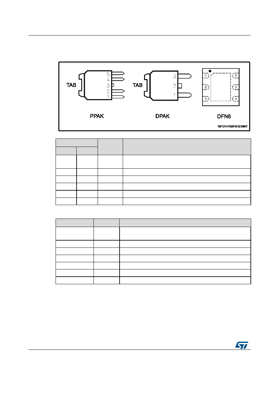 Pin configuration LDF 4/33 DocID025502 Rev 2 2 Pin configuration Figure 2: Pin connection (top view) Table 1: DPAK, PPAK pin description Pin n° Symbol Function PPAK DPAK 5 - ADJ/PG For adjustable versions: error amplifier input pin For fixed versions: power-good output 2 1 VIN Input voltage 4 3 VOUT Output voltage 1 - EN Enable pin logic input: low = shutdown, high = active 3 2 GND Ground TAB TAB GND Ground Table 2: DFN6-2x2 and 3x3 pin description Pin n° Symbol Function 2 ADJ/NC For adjustable versions: error amplifier input pin For fixed versions: not connected 6 VIN Input voltage 1 VOUT Output voltage 5 EN Enable pin logic input: low = shutdown, high = active 3 PG Power-good output 4 GND Ground Exposed pad GND Ground |
|
Enlace URL |
| ¿ALLDATASHEET es útil para Ud.? [ DONATE ] |
Todo acerca de Alldatasheet | Publicidad | Contáctenos | Política de Privacidad | Enlace a la hoja de datos | Intercambio de Enlaces | Lista de Fabricantes All Rights Reserved©Alldatasheet.com |
| Russian : Alldatasheetru.com | Korean : Alldatasheet.co.kr | Spanish : Alldatasheet.es | French : Alldatasheet.fr | Italian : Alldatasheetit.com Portuguese : Alldatasheetpt.com | Polish : Alldatasheet.pl | Vietnamese : Alldatasheet.vn Indian : Alldatasheet.in | Mexican : Alldatasheet.com.mx | British : Alldatasheet.co.uk | New Zealand : Alldatasheet.co.nz |
|
Family Site : ic2ic.com |
icmetro.com |
 Mexican ▼
 English
 Chinese
 German
 Japanese
 Russian
 Korean
 Spanish
 French
 Italian
 Portuguese
 Polish
 Vietnamese
 Indian
 Mexican
 British
 New Zealand


