 |
Motor de Búsqueda de Datasheet de Componentes Electrónicos |
|
|
Motor de Búsqueda de Datasheet de Componentes Electrónicos |
|
The question interval is too short.
Please try again in a few seconds.

Hello, Please ask a question about LTC1589CG Datasheet
# Example questions:
➢ What are the two different scenarios described in note 12 that affect the maximum clock frequency, and how do they differ?
➢ What is the primary factor that limits the maximum clock frequency when using a continuous clock with data changing on the rising edge of sck?
➢ Note 13 states that two factors limit the maximum clock frequency for daisy chaining. what are these two factors?
| Part No. | LTC1589CG |
| Manufacturer | LINER |
| Size | 276 Kbytes |
| Pages | 16 pages |
| Description | 12-/14-/16-Bit SoftSpan DACs with Programmable Output Range |


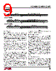
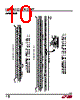


Okay, I've processed the provided text. Here's a summary and breakdown of the data, focusing on the timing parameters.
Overall Context:
This data describes the timing characteristics of a serial communication protocol, likely for a digital-to-analog converter (DAC) or a similar device from Analog Devices (LTC is a common prefix for their part numbers). It specifies how different signals need to be timed relative to each other to ensure correct data transfer.
Key Timing Parameters (from the extracted table):
Here's a breakdown of the timing parameters. I will not create a table, but rather describe them as a series of statements, given the layout of the original data.
️· t1 (Setup Time): This parameter dictates the minimum time the data must be stable *before* the clock signal arrives. This is crucial for the receiving device to reliably sample the data.
️· t2 (Hold Time): This parameter defines the minimum time the data must remain stable *after* the clock signal has passed. Like setup time, this ensures the data isn't corrupted by timing variations.
️· t3 (Clock High Time): Specifies the minimum duration that the clock signal must be high.
️· t4 (Clock Low Time): Specifies the minimum duration the clock signal must be low.
️· t5 (Cycle Time): Represents the total duration of one complete clock cycle (high time + low time).
️· t6 (Data Valid Time): Indicates the time after the clock edge when the data output is valid and can be read by the external circuitry.
️· t7 (Data Settling Time): The time required for the DAC output to settle to its final value after a new data word is loaded.
Frequency & Data Rate Implications:
️· Maximum Frequency (Data Rate): The timing parameters will directly influence the maximum frequency (or data rate) at which data can be reliably transferred. The tightest constraints (smallest hold and setup times) will limit the maximum frequency.
️· Daisy-Chaining: Note the mention of "daisy-chaining." If devices are connected in a chain, the timing constraints become even more critical, as the signal needs to propagate through multiple devices.
Important Notes:
️· Units: The provided data does *not* specify units (e.g., ns, µs). Without the units, the timing values are meaningless.
️· Temperature & Voltage: Timing characteristics can vary with temperature and supply voltage. The provided values are likely specified under certain operating conditions, and different conditions will require different timing margins.
️· Documentation: This extracted data is likely from a device datasheet. Always refer to the official datasheet for complete and accurate information.
If you can provide the units of measurement (ns, µs, etc.), I can offer more specific interpretations and calculations related to the maximum data rate. Also, tell me if you have any specific questions or calculations you want me to perform based on this data.
Overall Context:
This data describes the timing characteristics of a serial communication protocol, likely for a digital-to-analog converter (DAC) or a similar device from Analog Devices (LTC is a common prefix for their part numbers). It specifies how different signals need to be timed relative to each other to ensure correct data transfer.
Key Timing Parameters (from the extracted table):
️· t1 (Setup Time): This parameter dictates the minimum time the data must be stable *before* the clock signal arrives. This is crucial for the receiving device to reliably sample the data.
️· t2 (Hold Time): This parameter defines the minimum time the data must remain stable *after* the clock signal has passed. Like setup time, this ensures the data isn't corrupted by timing variations.
️· t3 (Clock High Time): Specifies the minimum duration that the clock signal must be high.
️· t4 (Clock Low Time): Specifies the minimum duration the clock signal must be low.
️· t5 (Cycle Time): Represents the total duration of one complete clock cycle (high time + low time).
️· t6 (Data Valid Time): Indicates the time after the clock edge when the data output is valid and can be read by the external circuitry.
️· t7 (Data Settling Time): The time required for the DAC output to settle to its final value after a new data word is loaded.
Frequency & Data Rate Implications:
️· Maximum Frequency (Data Rate): The timing parameters will directly influence the maximum frequency (or data rate) at which data can be reliably transferred. The tightest constraints (smallest hold and setup times) will limit the maximum frequency.
️· Daisy-Chaining: Note the mention of "daisy-chaining." If devices are connected in a chain, the timing constraints become even more critical, as the signal needs to propagate through multiple devices.
Important Notes:
️· Units: The provided data does *not* specify units (e.g., ns, µs). Without the units, the timing values are meaningless.
️· Temperature & Voltage: Timing characteristics can vary with temperature and supply voltage. The provided values are likely specified under certain operating conditions, and different conditions will require different timing margins.
️· Documentation: This extracted data is likely from a device datasheet. Always refer to the official datasheet for complete and accurate information.
| Part No. | LTC1589CG |
| Manufacturer | LINER |
| Size | 276 Kbytes |
| Pages | 16 pages |
| Description | 12-/14-/16-Bit SoftSpan DACs with Programmable Output Range |
| ¿ALLDATASHEET es útil para Ud.? [ DONATE ] |
Todo acerca de Alldatasheet | Publicidad | Contáctenos | Política de Privacidad | Enlace a la hoja de datos | Intercambio de Enlaces | Lista de Fabricantes All Rights Reserved©Alldatasheet.com |
| Russian : Alldatasheetru.com | Korean : Alldatasheet.co.kr | Spanish : Alldatasheet.es | French : Alldatasheet.fr | Italian : Alldatasheetit.com Portuguese : Alldatasheetpt.com | Polish : Alldatasheet.pl | Vietnamese : Alldatasheet.vn Indian : Alldatasheet.in | Mexican : Alldatasheet.com.mx | British : Alldatasheet.co.uk | New Zealand : Alldatasheet.co.nz |
|
Family Site : ic2ic.com |
icmetro.com |
 Mexican ▼
  English
 Chinese
 German
 Japanese
 Russian
 Korean
 Spanish
 French
 Italian
 Portuguese
 Polish
 Vietnamese
 Indian
 British
 New Zealand