|
Motor de Búsqueda de Datasheet de Componentes Electrónicos |
|
|
Motor de Búsqueda de Datasheet de Componentes Electrónicos |
|
LTC1589CG Datasheet(PDF) 9 Page - Linear Technology |
|
|
|||||||||||||||||||||||||||||
LTC1589CG Datasheet(HTML) 9 Page - Linear Technology |
|
|
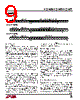
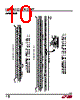
9 / 16 page  9 LTC1588/LTC1589/LTC1592 1588992fa OPERATIO Serial Interface When the CS/LD is brought to a logic low, the data on the SDI input is loaded into the shift register on the rising edge of the clock. A 4-bit command word (C3 C2 C1 C0), followed by four “don’t care” bits and 16 data bits (MSB-first) is the minimum loading sequence required for the LTC1588/LTC1589/LTC1592. When the CS/LD is brought to a logic high, the clock is disabled internally and the command word is executed. If no daisy-chaining is required, the input stream can be 24-bit wide as shown in Figure 1a. The first four bits are the command word, followed by four “don’t care” bits, then a 16-bit data word. The last four bits (LSBs) of this 16-bit data word are don’t cares for the LTC1588. For the LTC1589, the last 2 bits of the 16-bit data word are don’t cares. If daisy-chaining is required or the input needs to be written in two 16-bit wide segments, then the input stream must be 32-bit wide and the first 8 bits loaded are “don’t care” bits. The remaining bits work the same as a 24-bit stream which is described in the previous paragraph. The output of the internal 32-bit shift register is available on the SDO pin 32 clock cycles later. Multiple LTC1588/LTC1589/LTC1592s may be daisy- chained together by connecting the SDO pin to the SDI pin of the next IC. The clock and CS/LD signals should remain common to all ICs in the daisy-chain. The serial data is clocked to all ICs, then the CS/LD signal is pulled high to update all of them simultaneously. Power-On Reset and Clear When the power supply is first turned on, the LTC1588/ LTC1589/LTC1592 will power up in 5V unipolar mode (C3 C2 C1 C0 = 1000). All the internal registers are set to zeros and the DAC is set to zero code. The LTC1588/LTC1589/LTC1592 must first be pro- grammed in either unipolar or bipolar mode. There are six operating modes available and can be software-pro- grammed by the command word. When a CLR signal is brought to low, it clears all internal registers to zero. The DAC output voltage goes to zero volts. If an update DAC command (C3 C2 C1 C0 = 0001) is issued immediately after the CLR signal, the DAC output remains at zero volts. If a CLR signal is given within a 100ns interval immediately after CS/LD goes high, the user should reload the output range. Output Range Programming There are two output ranges available in unipolar mode and four output ranges available in bipolar mode. See Function Table for details. All output ranges are with re- spect to a 5V reference input. When changing the LTC1588/ LTC1589/LTC1592 to a new mode, the command word and data are given at the same time (24 or 32 bit). When C3 COMMAND DON’T CARE DATA (16 BITS) C2 C1 C0 X X X X D13 D14 D15 D12 D11 D10 D9 D8 D7 D6 D5 D4 D3 D2 D1 D0 1588992 TD2 MSB LSB C3 COMMAND DON’T CARE DATA (14 BITS + 2 DON’T-CARE BITS) C2 C1 C0 X X X X D13 D12 D11 D10 D9 D8 D7 D6 D5 D4 D3 D2 D1 D0 X X 1588992 TD3 MSB LSB C3 COMMAND DON’T CARE DATA (12 BITS + 4 DON’T-CARE BITS) C2 C1 C0 X X X X D11 D10 D9 D8 D7 D6 D5 D4 D3 D2 D1 D0 X X XX 1588992 TD4 MSB LSB INPUT WORD (LTC1592) INPUT WORD (LTC1589) INPUT WORD (LTC1588) |
|
|
Enlace URL |
| ¿ALLDATASHEET es útil para Ud.? [ DONATE ] |
Todo acerca de Alldatasheet | Publicidad | Contáctenos | Política de Privacidad | Enlace a la hoja de datos | Intercambio de Enlaces | Lista de Fabricantes All Rights Reserved©Alldatasheet.com |
| Russian : Alldatasheetru.com | Korean : Alldatasheet.co.kr | Spanish : Alldatasheet.es | French : Alldatasheet.fr | Italian : Alldatasheetit.com Portuguese : Alldatasheetpt.com | Polish : Alldatasheet.pl | Vietnamese : Alldatasheet.vn Indian : Alldatasheet.in | Mexican : Alldatasheet.com.mx | British : Alldatasheet.co.uk | New Zealand : Alldatasheet.co.nz |
|
Family Site : ic2ic.com |
icmetro.com |
 Mexican ▼
 English
 Chinese
 German
 Japanese
 Russian
 Korean
 Spanish
 French
 Italian
 Portuguese
 Polish
 Vietnamese
 Indian
 Mexican
 British
 New Zealand