|
Motor de Búsqueda de Datasheet de Componentes Electrónicos |
|
|
Motor de Búsqueda de Datasheet de Componentes Electrónicos |
|
LTC1589CG Datasheet(PDF) 7 Page - Linear Technology |
|
|
|||||||||||||||||||||||||||||
LTC1589CG Datasheet(HTML) 7 Page - Linear Technology |
|
|
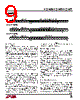
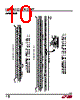
7 / 16 page  7 LTC1588/LTC1589/LTC1592 1588992fa IOUT1 (Pin 5): True DAC Current Output. Tied to the inverting input of the current-to-voltage op amp. IOUT2 (Pin 6): Complement of DAC Current Output. Nor- mally tied to AGND pin. AGND (Pin 7): Analog Ground. Tie to the system’s analog ground plane. GND (Pin 8): Ground. Tie to the system’s analog ground plane. VCC (Pin 9): Positive Supply Input. 4.5V ≤ VCC ≥ 5.5V. Requires a 0.1 µF bypass capacitor to ground. SDO (Pin 10): Serial Data Output. Data at this pin is shifted out on the rising edge of SCK. SDI (Pin 11): Serial Data Input. PI FU CTIO S FU CTIO TABLE Table 1 C3 0 0 0 0 0 0 0 0 1 1 1 1 1 1 1 1 C2 0 0 0 0 1 1 1 1 0 0 0 0 1 1 1 1 C1 0 0 1 1 0 0 1 1 0 0 1 1 0 0 1 1 C0 0 1 0 1 0 1 0 1 0 1 0 1 0 1 0 1 SREG DATA WORD Dn IN INPUT SHIFT REGISTER Dn X Dn Dn Dn Dn Dn Dn Dn X BUF1 INPUT BUFFER Dn Dn Dn Dn Dn Dn Dn Dn Dn No Change DAC OUTPUT RANGE No Change No Change No Change 5V 10V ±5V ±10V ±2.5V –2.5V to 7.5V No Change BUF2 DAC BUFFER (DAC OUTPUT) No Change Dn Dn Dn Dn Dn Dn Dn Dn No Change Copy Data Word Dn in SReg to Buf1 Copy the Data in Buf1 to Buf2 Copy Data Word Dn in SReg to Buf1 and Buf2 Reserved (Do Not Use) Reserved (Do Not Use) Reserved (Do Not Use) Reserved (Do Not Use) Reserved (Do Not Use) Set Range to 5V. Copy Dn in SReg to Buf1 and Buf2 Set Range to 10V. Copy Dn in SReg to Buf1 and Buf2 Set Range to ±5V. Copy Dn in SReg to Buf1 and Buf2 Set Range to ±10V. Copy Dn in SReg to Buf1 and Buf2 Set Range to ±2.5V. Copy Dn in SReg to Buf1 and Buf2 Set Range to –2.5V to 7V. Copy Dn in SReg to Buf1 and Buf2 Reserved (Do Not Use) No Operation Internal Register Status OPERATION EACH COMMAND IS EXECUTED ON THE RISING EDGE OF CS/LD COMMAND Data Word Dn (n = 0 to 15) is the last 16 bits shifted into the input shift register SReg that corresponds to the DAC code. SCK (Pin 12): Serial Interface Clock. Data on the SDI pin is shifted into the input shift register on rising edge of SCK. CS/LD (Pin 13): Chip Select Input. When CS/LD is low, SCK is enabled for shifting data into the input shift register. When CS/LD is pulled high, SCK is disabled and the control logic executes the control word (the first 4 bits of the input data stream as shown in Table 1). CLR (Pin 14): When CLR is taken to a logic low, it sets the DAC output to 0V and all internal registers to zero code. REF (Pin 15): DAC Reference Input. Typically 5V, accepts up to ±15V. R2 (Pin 16): Bipolar Resistor R2. Normally tied to the DAC reference input REF (Pin 15) and the output of the inverting amplifier tied to RCOM (Pin 1). |
|
|
Enlace URL |
| ¿ALLDATASHEET es útil para Ud.? [ DONATE ] |
Todo acerca de Alldatasheet | Publicidad | Contáctenos | Política de Privacidad | Enlace a la hoja de datos | Intercambio de Enlaces | Lista de Fabricantes All Rights Reserved©Alldatasheet.com |
| Russian : Alldatasheetru.com | Korean : Alldatasheet.co.kr | Spanish : Alldatasheet.es | French : Alldatasheet.fr | Italian : Alldatasheetit.com Portuguese : Alldatasheetpt.com | Polish : Alldatasheet.pl | Vietnamese : Alldatasheet.vn Indian : Alldatasheet.in | Mexican : Alldatasheet.com.mx | British : Alldatasheet.co.uk | New Zealand : Alldatasheet.co.nz |
|
Family Site : ic2ic.com |
icmetro.com |
 Mexican ▼
 English
 Chinese
 German
 Japanese
 Russian
 Korean
 Spanish
 French
 Italian
 Portuguese
 Polish
 Vietnamese
 Indian
 Mexican
 British
 New Zealand