 |
Motor de Búsqueda de Datasheet de Componentes Electrónicos |
|
|
Motor de Búsqueda de Datasheet de Componentes Electrónicos |
|
The question interval is too short.
Please try again in a few seconds.

Hello, Please ask a question about ICS2510C Datasheet
# Example questions:
➢ What are the minimum and maximum values for the 'a2' dimension of the ics2510c package in both millimeters and inches?
➢ What is the maximum allowable cycle-to-cycle jitter (tcyc-cyc) at a clock frequency of 133 mhz with loaded outputs?
➢ What is the typical operating current (idd1) of the ics2510c when cl = 0 pf and fin is at 66mhz?
| Part No. | ICS2510C |
| Manufacturer | IDT |
| Size | 86 Kbytes |
| Pages | 7 pages |
| Description | Distributes one clock input to one bank of ten outputs |


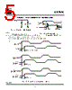
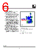
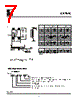

1. Device Information
️· Device: ICS2510C
️· Type: Clock Driver/Fanout Buffer
2. Package and Dimensions
️· Package Type: SOIC (likely a 24-pin SOIC) – Note the dimensions provided are for a 24-pin package
️· Dimensions (in mm and inches):
- A: 1.20 mm (Max)
- A1: 0.05 mm
- A2: 0.80 - 1.05 mm
- b: 0.19 - 0.30 mm
- c: 0.09 - 0.20 mm
- D: 7.70 - 7.90 mm
- E: 6.40 mm (Basic)
- E1: 4.30 - 4.50 mm
- e: 0.65 mm (Basic)
- L: 0.45 - 0.75 mm
- N: See Variations (This implies that the number of pins or other parameters related to pin arrangement might vary based on specific configurations.)
- α: 0° - 8°
- aaa: 0.10 mm
3. Electrical Characteristics
This section details a large number of electrical parameters. I'm going to group them into functional categories and provide a summary with key values. *Note: Values are "typical" unless otherwise noted.*
️· Output Characteristics:
- Output Impedance (RDSP): 36 Ω
- Output Impedance (RDSN): 32 Ω
- Output High Voltage (VOH): 2.4 - 2.9 V
- Output Low Voltage (VOL): 0.25 - 0.4 V
- Output High Current (IOH): -26 to -13.6 mA
- Output Low Current (IOL): 19 - 25 mA
- Rise Time (Tr): 0.5 - 2.1 ns
- Fall Time (Tf): 0.5 - 2.7 ns
- Duty Cycle: 45 - 55%
️· Jitter:
- Cycle-to-Cycle Jitter: Up to 75 ps at 133 MHz
- Absolute Jitter: Up to 57 ps
- Skew: Up to 150 ps
- Phase Error Jitter: Up to 50 ps
️· Input Characteristics:
- Input High Voltage (VIH): 2 V
- Input Low Voltage (VIL): 0.8 V
- Input High Current (IIH): 0.1 uA
- Input Low Current (IIL): 19 uA
- Input Capacitance: 4 pF
️· Power and Current:
- Operating Current (IDD1): 140 - 170 mA
️· Clock Frequency
- Fclk: 25 - 175 MHz
4. Functional Description (Implied from Tables)
️· Input Signals: CLKN, AVCC, OE (Output Enable)
️· Outputs: CLK(9:0) (likely clock outputs 0 through 9), FBOUT, Source
️· Functionality:
- The device is a clock fanout buffer, distributing a single clock input to multiple outputs.
- It has output enable functionality (OE) to disable the outputs.
- It has a shutdown function.
- The AVCC input is an analog power supply.
5. Variations
️· The document uses the term "SEE VARIATIONS" multiple times, particularly in the pin count and specific dimensions. This suggests there are different versions or options of this device with slightly different specifications or pinouts.
1. Device Information
️· Device: ICS2510C
️· Type: Clock Driver/Fanout Buffer
2. Package and Dimensions
️· Package Type: SOIC (likely a 24-pin SOIC) – Note the dimensions provided are for a 24-pin package
️· Dimensions (in mm and inches):
- A: 1.20 mm (Max)
- A1: 0.05 mm
- A2: 0.80 - 1.05 mm
- b: 0.19 - 0.30 mm
- c: 0.09 - 0.20 mm
- D: 7.70 - 7.90 mm
- E: 6.40 mm (Basic)
- E1: 4.30 - 4.50 mm
- e: 0.65 mm (Basic)
- L: 0.45 - 0.75 mm
- N: See Variations (This implies that the number of pins or other parameters related to pin arrangement might vary based on specific configurations.)
- α: 0° - 8°
- aaa: 0.10 mm
3. Electrical Characteristics
This section details a large number of electrical parameters. I'm going to group them into functional categories and provide a summary with key values. *Note: Values are "typical" unless otherwise noted.*
️· Output Characteristics:
- Output Impedance (RDSP): 36 Ω
- Output Impedance (RDSN): 32 Ω
- Output High Voltage (VOH): 2.4 - 2.9 V
- Output Low Voltage (VOL): 0.25 - 0.4 V
- Output High Current (IOH): -26 to -13.6 mA
- Output Low Current (IOL): 19 - 25 mA
- Rise Time (Tr): 0.5 - 2.1 ns
- Fall Time (Tf): 0.5 - 2.7 ns
- Duty Cycle: 45 - 55%
️· Jitter:
- Cycle-to-Cycle Jitter: Up to 75 ps at 133 MHz
- Absolute Jitter: Up to 57 ps
- Skew: Up to 150 ps
- Phase Error Jitter: Up to 50 ps
️· Input Characteristics:
- Input High Voltage (VIH): 2 V
- Input Low Voltage (VIL): 0.8 V
- Input High Current (IIH): 0.1 uA
- Input Low Current (IIL): 19 uA
- Input Capacitance: 4 pF
️· Power and Current:
- Operating Current (IDD1): 140 - 170 mA
️· Clock Frequency
- Fclk: 25 - 175 MHz
4. Functional Description (Implied from Tables)
️· Input Signals: CLKN, AVCC, OE (Output Enable)
️· Outputs: CLK(9:0) (likely clock outputs 0 through 9), FBOUT, Source
️· Functionality:
- The device is a clock fanout buffer, distributing a single clock input to multiple outputs.
- It has output enable functionality (OE) to disable the outputs.
- It has a shutdown function.
- The AVCC input is an analog power supply.
5. Variations
️· The document uses the term "SEE VARIATIONS" multiple times, particularly in the pin count and specific dimensions. This suggests there are different versions or options of this device with slightly different specifications or pinouts.
| Part No. | ICS2510C |
| Manufacturer | IDT |
| Size | 86 Kbytes |
| Pages | 7 pages |
| Description | Distributes one clock input to one bank of ten outputs |
| ¿ALLDATASHEET es útil para Ud.? [ DONATE ] |
Todo acerca de Alldatasheet | Publicidad | Contáctenos | Política de Privacidad | Enlace a la hoja de datos | Intercambio de Enlaces | Lista de Fabricantes All Rights Reserved©Alldatasheet.com |
| Russian : Alldatasheetru.com | Korean : Alldatasheet.co.kr | Spanish : Alldatasheet.es | French : Alldatasheet.fr | Italian : Alldatasheetit.com Portuguese : Alldatasheetpt.com | Polish : Alldatasheet.pl | Vietnamese : Alldatasheet.vn Indian : Alldatasheet.in | Mexican : Alldatasheet.com.mx | British : Alldatasheet.co.uk | New Zealand : Alldatasheet.co.nz |
|
Family Site : ic2ic.com |
icmetro.com |
 Mexican ▼
  English
 Chinese
 German
 Japanese
 Russian
 Korean
 Spanish
 French
 Italian
 Portuguese
 Polish
 Vietnamese
 Indian
 British
 New Zealand