|
Motor de Búsqueda de Datasheet de Componentes Electrónicos |
|
|
Motor de Búsqueda de Datasheet de Componentes Electrónicos |
|
ICS2510C Datasheet(PDF) 6 Page - Integrated Device Technology |
|
|
|||||||||||||||||||||||||||||
ICS2510C Datasheet(HTML) 6 Page - Integrated Device Technology |
|
|
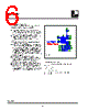
6 / 7 page  6 ICS2510C 0010G—09/22/09 General Layout Precautions: An ICS2509C is used as an example. It is similar to the ICS2510C. The same rules and methods apply. 1) Use copper flooded ground on the top signal layer under the clock buffer The area under U1 in figure 1 on the right is an example. Every ground pin goes to a ground via. The vias are not visible in figure 1. 2) Use power vias for power and ground. Vias 20 mil or larger in diameter have lower high frequency impedance. Vias for signals may be minimum drill size. 3) Make all power and ground traces are as wide as the via pad for lower inductance. 4) VAA for pin 23 has a low pass RC filter to decouple the digital and analog supplies. C9-12 may be replaced with a single low ESR (0.8 ohm or less) device with the same total capacitance. R2 may be replaced with a ferrite bead. The bead should have a DC resistance of at least 0.5 ohms. 1 ohm is better. It should have an impedance of at least 300 ohms at 100MHz. 600 ohms at 100MHz is better. 5) Notice that ground vias are never shared. 6) All VCC pins have a decoupling capacitor. Power is always routed from the plane connection via to the capacitor pad to the VCC pin on the clock buffer. 7) Component R1 is located at the clock source. 8) Component C1, if used, has the effect of adding delay. 9) Component C7 , if used, has the effect of subtracting delay. Delaying the FBIn clock will cause the output clocks to be earlier. A more effective method is to use the propagation time of a trace between FBOut and FBIn. Component Values: C1,C7= As necessary for delay adjust C[6:2]=.01uF C8,C13=0.1uF C[12:9]=4.7Uf R1=10 ohm. Locate at driver R2=10 ohm. Figure 1. |
|
|
Enlace URL |
| ¿ALLDATASHEET es útil para Ud.? [ DONATE ] |
Todo acerca de Alldatasheet | Publicidad | Contáctenos | Política de Privacidad | Enlace a la hoja de datos | Intercambio de Enlaces | Lista de Fabricantes All Rights Reserved©Alldatasheet.com |
| Russian : Alldatasheetru.com | Korean : Alldatasheet.co.kr | Spanish : Alldatasheet.es | French : Alldatasheet.fr | Italian : Alldatasheetit.com Portuguese : Alldatasheetpt.com | Polish : Alldatasheet.pl | Vietnamese : Alldatasheet.vn Indian : Alldatasheet.in | Mexican : Alldatasheet.com.mx | British : Alldatasheet.co.uk | New Zealand : Alldatasheet.co.nz |
|
Family Site : ic2ic.com |
icmetro.com |
 Mexican ▼
 English
 Chinese
 German
 Japanese
 Russian
 Korean
 Spanish
 French
 Italian
 Portuguese
 Polish
 Vietnamese
 Indian
 Mexican
 British
 New Zealand