|
Motor de Búsqueda de Datasheet de Componentes Electrónicos |
|
|
Motor de Búsqueda de Datasheet de Componentes Electrónicos |
|
LTM4650-1 Datasheet(PDF) 7 Page - Linear Technology |
|
|
|||||||||||||||||||||||||||||
LTM4650-1 Datasheet(HTML) 7 Page - Linear Technology |
|
|
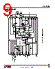
7 / 36 page  LTM4636 7 4636f For more information www.linear.com/LTM4636 pin FuncTions VOUT(A1-A12,B1-B12,C1-C12,D1-D2,D11-D12):Power OutputPins.ApplyoutputloadbetweenthesepinsandGND pins. Recommend placing output decoupling capacitance between these pins and GND pins. Review Table 4. MODE_PLLIN(H3):ForcedContinuousMode,BurstMode Operation, or Pulse-Skipping Mode Selection Pin and External Synchronization Input to Phase Detector Pin. Connect this pin to INTVCC to enable pulse-skipping mode ofoperation.Connecttogroundtoenableforcedcontinuous modeofoperation.FloatingthispinwillenableBurstMode operation. A clock on this pin will enable synchronization with forced continuous operation. See the Applications Information section. VOUTS1– (D3): VOUT Sense Ground for the Remote Sense Amplifier. This pin connects to the ground remote sense point. Connect to ground when not used. See the Applica- tions Information section. VOUTS1+ (D4): This pin should connect to VOUT and is connected to VFB through a 4.99k resistor. This pin is used to connect to a remote sense point of the load for accurate voltage sensing. Either connect to remote sense point or directly to VOUT. See the Applications Information section for details. COMPB(D5):Internalcompensationnetworkprovidedthat coincides with proper stability utilizing the values in Table 5. Just connect this pin to COMPA for internal compensa- tion. In parallel operation with other LTM4636 devices, connect COMPA and COMPB pins together for internal compensation, then connect all COMPA pins together. GND (D6-D10, E6-E10, E12, F7, F8, F10-F12, G1-G2, G6 G10, H1, H10-H12, J1-J3, J8-J12, K1-K3, K9-K10, K12, L1-L3, L9-L10, L12, M1-M3, M9-M12): Ground Pins for Both Input and Output Returns. PGOOD(E1):OutputVoltagePowerGoodIndicator.Open- drain logic output is pulled to ground when the output voltage exceeds a ±7.5% regulation window. RUNC (E2): Run Control Pin. A voltage above 1.35V will turn on the control section of the module. A 10k resistor to ground is internal to the module for setting the RUN pin threshold with a resistor to 5V, and allowing a pull- up resistor to PVCC for enabling the device. See Figure 1 Block Diagram. TRACK/SS(E3):OutputVoltageTrackingPinandSoft-Start Inputs. The pin has a 1.25µA pull-up current source. A capacitor from this pin to ground will set a soft-start ramp rate. In tracking, the regulator output can be tracked to a differentvoltage.Thedifferentvoltageisappliedtoavoltage divider then to the slave output’s track pin. This voltage divider is equal to the slave output’s feedback divider for coincidental tracking. Default soft-start of 750µs with TRACK/SS pin connected to INTVCC pin. See the Applica- tions Information section. In PolyPhase® applications tie the TRACK/SS pins together. VFB (E4): The Negative Input of the Error Amplifier. Inter- nally,thispinisconnectedtoVOUTS1witha4.99kprecision resistor. Different output voltages can be programmed with an additional resistor between VFB and VOUTS1–. In PolyPhaseoperation,tyingtheVFBpinstogetherallowsfor paralleloperation.SeetheApplicationsInformationsection. COMPA(E5):CurrentControlThresholdandErrorAmplifier Compensation Point. The current comparator threshold increases with this control voltage. Tie all COMPA pins together for parallel operation. This pin allows external compensation. See the Applications Information section. SNSP2 (F1): Current Sense Signal Path. Connect this pin to SNSP1 (F2). SNSP1 (F2): Current Sense Signal Path. Connect this pin to SNSP2 (F1). Both pins are used to calibrate current sense matching and current limit at final test. HIZREG (F3): When this pin is pulled low the power stage is disabled into high impedance. Tie this pin to VIN or in TVCC for normal operation. PACKAGE ROW AND COLUMN LABELING MAY VARY AMONG µModule PRODUCTS. REVIEW EACH PACKAGE LAYOUT CAREFULLY. |
|
Enlace URL |
| ¿ALLDATASHEET es útil para Ud.? [ DONATE ] |
Todo acerca de Alldatasheet | Publicidad | Contáctenos | Política de Privacidad | Enlace a la hoja de datos | Intercambio de Enlaces | Lista de Fabricantes All Rights Reserved©Alldatasheet.com |
| Russian : Alldatasheetru.com | Korean : Alldatasheet.co.kr | Spanish : Alldatasheet.es | French : Alldatasheet.fr | Italian : Alldatasheetit.com Portuguese : Alldatasheetpt.com | Polish : Alldatasheet.pl | Vietnamese : Alldatasheet.vn Indian : Alldatasheet.in | Mexican : Alldatasheet.com.mx | British : Alldatasheet.co.uk | New Zealand : Alldatasheet.co.nz |
|
Family Site : ic2ic.com |
icmetro.com |
 Mexican ▼
 English
 Chinese
 German
 Japanese
 Russian
 Korean
 Spanish
 French
 Italian
 Portuguese
 Polish
 Vietnamese
 Indian
 Mexican
 British
 New Zealand