|
Motor de Búsqueda de Datasheet de Componentes Electrónicos |
|
|
Motor de Búsqueda de Datasheet de Componentes Electrónicos |
|
LTM4650-1 Datasheet(PDF) 8 Page - Linear Technology |
|
|
|||||||||||||||||||||||||||||
LTM4650-1 Datasheet(HTML) 8 Page - Linear Technology |
|
|
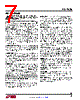
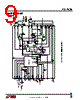
8 / 36 page  LTM4636 8 4636f For more information www.linear.com/LTM4636 pin FuncTions SGND(F4,G4):SignalGroundPin.Returngroundpathfor all analog and low power circuitry. Tie a single connection to the output capacitor GND in the application. See layout guidelines in Figure 18. INTVCC (F6): Internal 5.5V LDO for Driving the Control CircuitryintheLTM4636.INTVCCiscontrolledandenabled when RUNC is activated high. Tie to VIN, when 4.7V ≤ VIN ≤ 5.5V, minimum VIN = 4.2V. FREQ (G5): A resistor can be applied from this pin to ground to set the operating frequency. This pin sources 20µA. See the Applications Information section. PHASMD (G7): This pin can be voltage programmed to change the phase relationship of the CLKOUT pin with reference to the internal clock or an input synchronized clock. The INTVCC (5.5V) output can be voltage divided down to the PHASMD pin to set the particular phase. The Electrical Characteristics show the different settings to select a particular phase. See the Applications Informa- tion section. RUNP (G8): This pin enables the PVCC supply. This pin can be connected to VIN, or tie to ground when connecting PVCC to VIN ≤ 5.5V. RUNP needs to sequence up before RUNC. A 15k resistor from PVCC to RUNC with a 0.1µF capacitor will provide enough delay. In parallel operation with multiple LTM4636s, the resistor can be reduced in value by N times and the 0.1µF can be increased N times. SeeApplicationsInformationsection.RUNPcanbeusedto settheminimumUVLOwithavoltagedivider.SeeFigure1. NC (G9): No Connection. PVCC (F9): 5V Power Output and Power for Internal Power MOSFETDrivers.Theregulatorcanpower50mAofexternal sourcing for additional use. Place a 22µF ceramic filter capacitor on this pin to ground. When VIN < 5.5V, tie VIN and PVCC together along with INTVCC. Then tie RUNP to GND. If VIN > 5.5V then operate PVCC regulator as normal. See the Typical Application examples. TEMP+ (G12): Temperature Monitor. An internal diode connected NPN transistor. See the Applications Informa- tion section. TEMP– (G11): Low Side of the Internal Temperature Monitor. CLKOUT (G3): Clock out signal that can be phase selected to the main internal clock or synchronized clock using the PHASMD pin. CLKOUT can be used for multiphase applications. See the Applications Information section. TEST1(H4),TEST2(F5),TEST3(H2),TEST4(E11),GMON (H9):These are test pins used in the final production test of the part. Leave floating. VIN (H5-H6, J4-J7, K4-K8, L4-L8, M4-M8): Power Input Pins. Apply input voltage between these pins and GND pins. Recommend placing input decoupling capacitance directly between VIN and GND pins. PWM (H7): PWM output that drives the power stage. Primarily used for test, but can be monitored in debug or testing. TMON(H8):TemperatureMonitorPin.Internaltemperature monitor,variesfrom1Vat25°Cto1.44Vat150°C,disables power stage at 150°C. If this feature is not desired, then tie the TMON pin to GND. SW (L11, K11): These are pin connections to the internal switch node for test evaluation and monitoring. An R-C snubber can be placed from the switch pins to GND to eliminate any high frequency ringing. See the Applications Information section. |
|
Enlace URL |
| ¿ALLDATASHEET es útil para Ud.? [ DONATE ] |
Todo acerca de Alldatasheet | Publicidad | Contáctenos | Política de Privacidad | Enlace a la hoja de datos | Intercambio de Enlaces | Lista de Fabricantes All Rights Reserved©Alldatasheet.com |
| Russian : Alldatasheetru.com | Korean : Alldatasheet.co.kr | Spanish : Alldatasheet.es | French : Alldatasheet.fr | Italian : Alldatasheetit.com Portuguese : Alldatasheetpt.com | Polish : Alldatasheet.pl | Vietnamese : Alldatasheet.vn Indian : Alldatasheet.in | Mexican : Alldatasheet.com.mx | British : Alldatasheet.co.uk | New Zealand : Alldatasheet.co.nz |
|
Family Site : ic2ic.com |
icmetro.com |
 Mexican ▼
 English
 Chinese
 German
 Japanese
 Russian
 Korean
 Spanish
 French
 Italian
 Portuguese
 Polish
 Vietnamese
 Indian
 Mexican
 British
 New Zealand