|
Motor de Búsqueda de Datasheet de Componentes Electrónicos |
|
|
Motor de Búsqueda de Datasheet de Componentes Electrónicos |
|
MSM65522 Datasheet(PDF) 7 Page - OKI electronic componets |
|
|
|||||||||||||||||||||||||||||
MSM65522 Datasheet(HTML) 7 Page - OKI electronic componets |
|
|
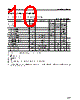
7 / 22 page  7/22 ¡ Semiconductor MSM65522/65P522 Secondary Functions Function Symbol Type Description Serial Port RXD I/O P2.0 secondary functions. UART: Input pin for a synchronous communication receive data. Synchronous: Input/output pin for serial port transmit/receive data. TXD O P2.1 secondary functions. UART: Input pin for a synchronous communication receive data. Synchronous: Output pin for serial port synchronizing clock. External interrupt INT0 I Secondary function of P2.2 input pin for external interrupt 0. The interrupt can be triggered by the rising edge, falling edge, or both edges of rising or falling. INT1/Gate I Secondary function of P2.3 input pin for external interrupt 1. The interrupt can be triggered by the rising edge, falling edge, or both rising and falling edges. Also used as a gate signal input pin for gating the counter of timer 0. INT2 I Secondary function of P3.4 input pin for external interrupt 2. The interrupt can be triggered by the rising edge, falling edge, or both rising and falling edges. HSTOP I Secondary function of P2.0 input pin for hardware stop mode. If this pin goes low while the HSTP bit in SBYCON is set to 1, the chip enters hard stop mode. In hardware stop mode the clock stops and the CPU and on-chip peripheral functions shut down to conserve power. Control SFTO O Shift Registers P3.5 secondary functions. Shift register data output pin. SFTI I P3.6 secondary functions. Shift register data output pin. SFTCK I/O P3.7 secondary functions. Shift register synchronizing clock input/output pin. In master mode: clock output In slave mode: clock input T0CK I Secondary function of P2.4: external clock input pin for timer 0. Timer 0 T1OUT O Secondary function of P2.7: outputs a waveform with twice the cycle of the overflow interval of timer 1. Timer 1 AI0 to AI7 O Secondary function of P6.0 to P6.7: functions as analog input channel in A/D conversion. A/D Converter |
|
|
Enlace URL |
| ¿ALLDATASHEET es útil para Ud.? [ DONATE ] |
Todo acerca de Alldatasheet | Publicidad | Contáctenos | Política de Privacidad | Enlace a la hoja de datos | Intercambio de Enlaces | Lista de Fabricantes All Rights Reserved©Alldatasheet.com |
| Russian : Alldatasheetru.com | Korean : Alldatasheet.co.kr | Spanish : Alldatasheet.es | French : Alldatasheet.fr | Italian : Alldatasheetit.com Portuguese : Alldatasheetpt.com | Polish : Alldatasheet.pl | Vietnamese : Alldatasheet.vn Indian : Alldatasheet.in | Mexican : Alldatasheet.com.mx | British : Alldatasheet.co.uk | New Zealand : Alldatasheet.co.nz |
|
Family Site : ic2ic.com |
icmetro.com |
 Mexican ▼
 English
 Chinese
 German
 Japanese
 Russian
 Korean
 Spanish
 French
 Italian
 Portuguese
 Polish
 Vietnamese
 Indian
 Mexican
 British
 New Zealand