 |
Motor de Búsqueda de Datasheet de Componentes Electrónicos |
|
|
Motor de Búsqueda de Datasheet de Componentes Electrónicos |
|
ADP2165ACPZ-R7 Datasheet(PDF) 15 Page - Analog Devices |
|
|
|||||||||||||||||||||||||||||
ADP2165ACPZ-R7 Datasheet(HTML) 15 Page - Analog Devices |
|
|
15 / 23 page 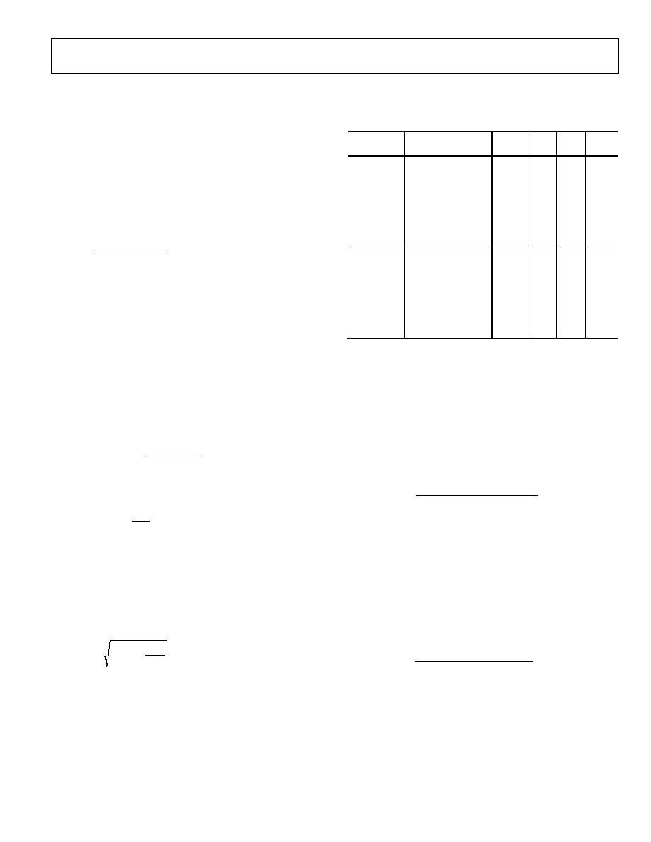 Data Sheet ADP2165/ADP2166 Rev. B | Page 15 of 23 INDUCTOR SELECTION The inductor value is determined by the operating frequency, input voltage, output voltage, and inductor ripple current. Using a small inductor leads to a faster transient response; however, it degrades efficiency due to a larger inductor ripple current. Conversely, using a large inductor value leads to a smaller ripple current and better efficiency; however, it results in a slower transient response. As a guideline, the inductor ripple current, ΔIL, is typically set to one-third of the maximum load current. The inductor value is calculated using the following equation: L = SW L OUT PVIN f I D V V × ∆ × − ) ( where: VPVIN is the input voltage. VOUT is the output voltage. ΔIL is the inductor ripple current. fSW is the switching frequency. D is the duty cycle, D = VOUT/VPVIN. The ADP2165/ADP2166 use adaptive slope compensation in the current loop to prevent subharmonic oscillations when the duty cycle is larger than 50%. The internal slope compensation limits the minimum inductor value. For a duty cycle that is larger than 50%, the minimum inductor value is determined by using the following equation: L (Minimum) = SW OUT f D V × − × 4 ) 1 ( The peak inductor current is calculated by using the following equation: IPEAK = IOUT + 2 L I ∆ The saturation current of the inductor must be larger than the peak inductor current. For ferrite core inductors with a quick saturation characteristic, the saturation current rating of the inductor must be higher than the current limit threshold of the switch. This prevents the inductor from reaching saturation. The rms current of the inductor is calculated from the following equation: IRMS = 12 2 2 L OUT I I ∆ + Shielded ferrite core materials are recommended for low core loss and low EMI. Table 6 lists some recommended inductors. Table 6. Recommended Inductors Vendor Part No. L (µH) ISAT (A) IRMS (A) DCR (mΩ) Würth Elektronik 744311022 0.22 32 21 1.10 744314047 0.47 20 18 1.35 744314076 0.76 15 15.5 2.25 744311100 1.0 19 15 4.6 744311150 1.5 14 11 6.6 7443340220 2.2 12.5 16.5 4.4 7443340330 3.3 8.5 14 6.5 Coilcraft XAL7020-271ME 0.27 30 21 2.9 XAL7020-331ME 0.33 28 20 4.0 XAL7020-471ME 0.47 24.3 17 4.75 XAL7020-681ME 0.68 22.3 13 7.9 XAL7020-102ME 1.0 16.4 11 9.8 XAL7030-152ME 1.5 23.5 15 7.6 XAL7030-222ME 2.2 18 12.9 13.7 OUTPUT CAPACITOR SELECTION The output capacitor selection affects the output ripple voltage load step transient and the loop stability of the regulator. For example, during a load step transient where the load is suddenly increased, the output capacitor supplies the load until the control loop can ramp up the inductor current. The delay caused by the control loop causes the output to undershoot. The output capacitance that is required to satisfy the voltage droop requirement can be calculated by using the following equation: COUT_UV = UV OUT OUT PVIN STEP UV V V V L I K _ 2 ) ( 2 ∆ × − × × ∆ × where: KUV is a factor, with a typical setting of KUV = 2. ΔISTEP is the load step. ΔVOUT_UV is the allowable undershoot on the output voltage. Another example occurs when a load is suddenly removed from the output, and the energy stored in the inductor rushes into the output capacitor, causing the output to overshoot. The output capacitance that is required to meet the overshoot requirement can be calculated using the following equation: COUT_OV = 2 2 _ 2 ) ( OUT OV OUT OUT STEP OV V V V L I K − ∆ + × ∆ × where: KOV is a factor, with a typical setting of KOV = 2. ΔVOUT_OV is the allowable overshoot on the output voltage. |
|
|
Enlace URL |
| ¿ALLDATASHEET es útil para Ud.? [ DONATE ] |
Todo acerca de Alldatasheet | Publicidad | Contáctenos | Política de Privacidad | Enlace a la hoja de datos | Intercambio de Enlaces | Lista de Fabricantes All Rights Reserved©Alldatasheet.com |
| Russian : Alldatasheetru.com | Korean : Alldatasheet.co.kr | Spanish : Alldatasheet.es | French : Alldatasheet.fr | Italian : Alldatasheetit.com Portuguese : Alldatasheetpt.com | Polish : Alldatasheet.pl | Vietnamese : Alldatasheet.vn Indian : Alldatasheet.in | Mexican : Alldatasheet.com.mx | British : Alldatasheet.co.uk | New Zealand : Alldatasheet.co.nz |
|
Family Site : ic2ic.com |
icmetro.com |
 Mexican ▼
 English
 Chinese
 German
 Japanese
 Russian
 Korean
 Spanish
 French
 Italian
 Portuguese
 Polish
 Vietnamese
 Indian
 Mexican
 British
 New Zealand


