|
Motor de Búsqueda de Datasheet de Componentes Electrónicos |
|
|
Motor de Búsqueda de Datasheet de Componentes Electrónicos |
|
LT6003CDC Datasheet(PDF) 14 Page - Linear Technology |
|
|
|||||||||||||||||||||||||||||
LT6003CDC Datasheet(HTML) 14 Page - Linear Technology |
|
|
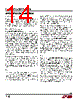
14 / 20 page  LT6003/LT6004/LT6005 14 600345f APPLICATIONS INFORMATION Supply Voltage The positive supply of the LT6003/LT6004/LT6005 should be bypassed with a small capacitor (about 0.01μF) within an inch of the pin. When driving heavy loads, an additional 4.7μFelectrolyticcapacitorshouldbeused.Whenusingsplit supplies, the same is true for the negative supply pin. Rail-to-Rail Characteristics The LT6003/LT6004/LT6005 are fully functional for an input signal range from the negative supply to the positive sup- ply. Figure 1 shows a simplified schematic of the amplifier. The input stage consists of two differential amplifiers, a PNP stage Q3/Q6 and an NPN stage Q4/ Q5 that are active over different ranges of the input common mode voltage. The PNP stage is active for common mode voltages, VCM, between the negative supply to approximately 0.9V below the positive supply. As VCM moves closer towards the positive supply, the transistor Q7 will steer Q2’s tail current to the current mirror Q8/Q9, activating the NPN differential pair. The PNP pair becomes inactive for the rest of the input common mode voltage range up to the positive supply. The second stage is a folded cascode and current mir- ror that converts the input stage differential signals into a single ended output. Capacitor C1 reduces the unity cross frequency and improves the frequency stability without degrading the gain bandwidth of the amplifier. The complementary drive generator supplies current to the output transistors that swing from rail to rail. Input Input bias current (IB) is minimized with cancellation circuitry on both input stages. The cancellation circuitry remains active when VCM is more than 300mV from either rail. As VCM approaches V – the cancellation circuitry turns off and IB is determined by the tail current of Q2 and the beta of the PNP input transistors. As VCM approaches V + devices in the cancellation circuitry saturate causing IB to increase (in the nanoamp range). Input offset voltage errors due to IB can be minimized by equalizing the noninverting and inverting source impedances. The input offset voltage changes depending on which input stage is active; input offset voltage is trimmed on both input stages, and is guaranteed to be 500μV max in the PNP stage. By trimming the input offset voltage of both input stages, the input offset voltage shift over the entire common mode range (CMRR) is typically 160μV, maintain- ing the precision characteristics of the amplifier. The input stage of the LT6003/LT6004/LT6005 incorpo- rates phase reversal protection to prevent wrong polarity outputs from occurring when the inputs are driven up to 9V below the negative rail. 600k protective resistors are included in the input leads so that current does not become excessive when the inputs are forced below V– or when a large differential signal is applied. Input current should be limited to 10mA when the inputs are driven above the positive rail. Output The output of the LT6003/LT6004/LT6005 is guaranteed to swing within 100mV of the positive rail and 50mV of the negative rail with no load, over the industrial temperature range. The LT6003/LT6004/LT6005 can typically source 8mA on a single 5V supply. Sourcing current is reduced to 5mA on a single 1.8V supply as noted in the electrical characteristics. However, when sourcing more than 250μA with an output load impedance greater than 20kΩ, a 1μF capacitor in series with a 2k resistor should be placed from the output to ground to insure stability. The normally reverse-biased substrate diode from the output to V– will cause unlimited currents to flow when the output is forced below V–. If the current is transient and limited to 100mA, no damage will occur. |
|
|
Enlace URL |
| ¿ALLDATASHEET es útil para Ud.? [ DONATE ] |
Todo acerca de Alldatasheet | Publicidad | Contáctenos | Política de Privacidad | Enlace a la hoja de datos | Intercambio de Enlaces | Lista de Fabricantes All Rights Reserved©Alldatasheet.com |
| Russian : Alldatasheetru.com | Korean : Alldatasheet.co.kr | Spanish : Alldatasheet.es | French : Alldatasheet.fr | Italian : Alldatasheetit.com Portuguese : Alldatasheetpt.com | Polish : Alldatasheet.pl | Vietnamese : Alldatasheet.vn Indian : Alldatasheet.in | Mexican : Alldatasheet.com.mx | British : Alldatasheet.co.uk | New Zealand : Alldatasheet.co.nz |
|
Family Site : ic2ic.com |
icmetro.com |
 Mexican ▼
 English
 Chinese
 German
 Japanese
 Russian
 Korean
 Spanish
 French
 Italian
 Portuguese
 Polish
 Vietnamese
 Indian
 Mexican
 British
 New Zealand