 |
Motor de Búsqueda de Datasheet de Componentes Electrónicos |
|
|
Motor de Búsqueda de Datasheet de Componentes Electrónicos |
|
STDRIVE101TR Datasheet(PDF) 21 Page - STMicroelectronics |
|
|
|||||||||||||||||||||||||||||
STDRIVE101TR Datasheet(HTML) 21 Page - STMicroelectronics |
|
|
21 / 32 page 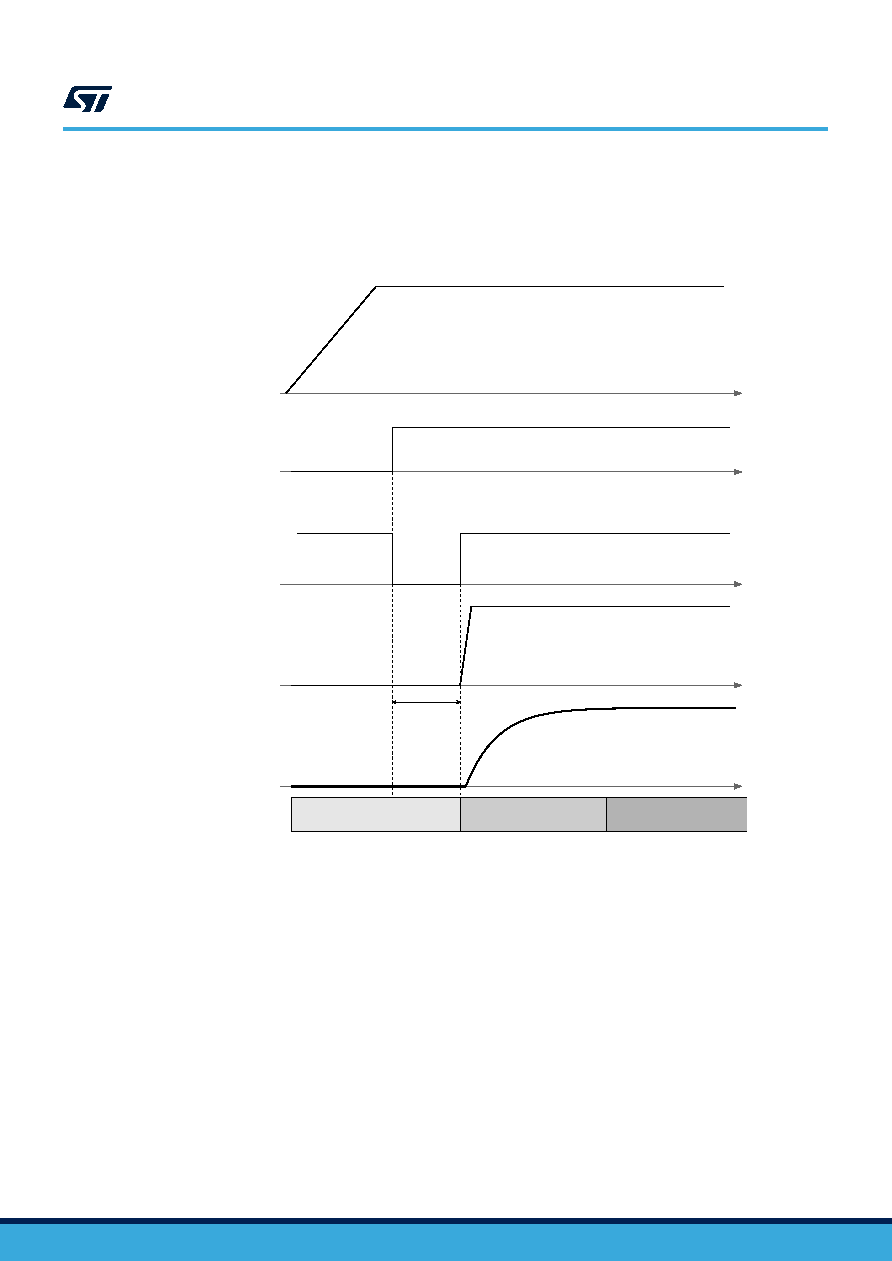 When the REG12 pin is supplied externally, the internal regulator is disabled. When leaving the standby condition raising one of the digital inputs, the nFAULT pin goes low, even if there is no UVLO condition on the REG12 pin, as shown in Figure 18 Figure 18. Power-up sequence, external supply on REG12 pin twake Vs/REG12 INLx/ENx nFAULT GLSx Standby Bootstrap cap. charge Operative VBOx Voltage on boot capacitor 5.6 VDS monitoring protection The device monitors the VDS of the power stage’s MOSFETs in order to detect anomalous conditions. The VDS of each MOSFET is compared to a reference threshold ( VDSth). The reference threshold is generated according to the voltage applied to the SCREF pin: Equation 6 (6) VDStℎ=VSCREF The SCREF voltage must be in the range between 0.2 V to VSCREF,en. If the voltage is above VSCREF,dis, the protection is disabled. When enabled, the protection triggers one of the following conditions occur: • GLSx output is high and VOUTx > VDSth for more than tDFSC STDRIVE101 VDS monitoring protection DS13472 - Rev 1 page 21/32 |
|
Enlace URL |
| ¿ALLDATASHEET es útil para Ud.? [ DONATE ] |
Todo acerca de Alldatasheet | Publicidad | Contáctenos | Política de Privacidad | Enlace a la hoja de datos | Intercambio de Enlaces | Lista de Fabricantes All Rights Reserved©Alldatasheet.com |
| Russian : Alldatasheetru.com | Korean : Alldatasheet.co.kr | Spanish : Alldatasheet.es | French : Alldatasheet.fr | Italian : Alldatasheetit.com Portuguese : Alldatasheetpt.com | Polish : Alldatasheet.pl | Vietnamese : Alldatasheet.vn Indian : Alldatasheet.in | Mexican : Alldatasheet.com.mx | British : Alldatasheet.co.uk | New Zealand : Alldatasheet.co.nz |
|
Family Site : ic2ic.com |
icmetro.com |
 Mexican ▼
 English
 Chinese
 German
 Japanese
 Russian
 Korean
 Spanish
 French
 Italian
 Portuguese
 Polish
 Vietnamese
 Indian
 Mexican
 British
 New Zealand


