 |
Motor de Búsqueda de Datasheet de Componentes Electrónicos |
|
|
Motor de Búsqueda de Datasheet de Componentes Electrónicos |
|
STPCATLAS Datasheet(PDF) 98 Page - STMicroelectronics |
|
|
|||||||||||||||||||||||||||||
STPCATLAS Datasheet(HTML) 98 Page - STMicroelectronics |
|
|
98 / 111 page 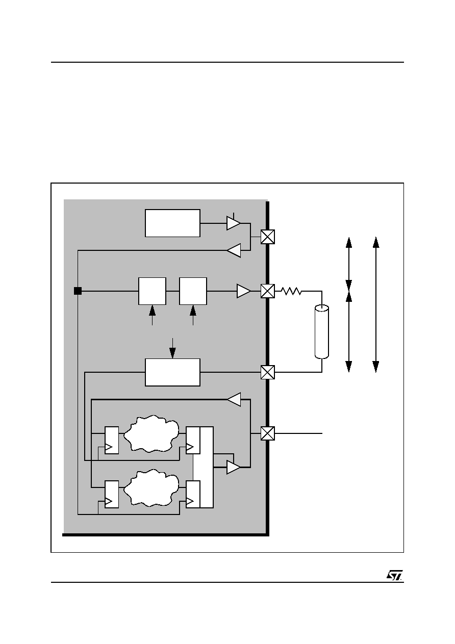 DESIGN GUIDELINES 98/111 Issue 1.0 - July 24, 2002 6.4.4. PCI INTERFACE 6.4.4.1. Introduction In order to achieve a PCI interface which work at clock frequencies up to 33MHz, careful consideration has to be given to the timing of the interface with all the various electrical and physical constraints taken into consideration. 6.4.4.2. PCI Clocking Scheme The PCI Clocking Scheme deserves a special mention here. Basically the PCI clock (PCICLKO) is generated on-chip from HCLK through a programmable delay line and a clock divider. The nominal frequency is 33MHz. This clock must be looped to PCICLKI and goes to the internal South Bridge through a deskewer. On the contrary, the internal North Bridge is clocked by HCLK, putting some additionnal constraints on T0 and T1. Figure 6-28. Clock Scheme HCLK PLL 1/2 1/3 1/4 clock Strap Options PCICLKO T1 PCICLKI HCLK AD[31:0] South North Deskewer MUX T0 T2 delay STPC MD[30:27] MD[17,4] MD[7:6] Bridge Bridge |
|
Enlace URL |
| ¿ALLDATASHEET es útil para Ud.? [ DONATE ] |
Todo acerca de Alldatasheet | Publicidad | Contáctenos | Política de Privacidad | Enlace a la hoja de datos | Intercambio de Enlaces | Lista de Fabricantes All Rights Reserved©Alldatasheet.com |
| Russian : Alldatasheetru.com | Korean : Alldatasheet.co.kr | Spanish : Alldatasheet.es | French : Alldatasheet.fr | Italian : Alldatasheetit.com Portuguese : Alldatasheetpt.com | Polish : Alldatasheet.pl | Vietnamese : Alldatasheet.vn Indian : Alldatasheet.in | Mexican : Alldatasheet.com.mx | British : Alldatasheet.co.uk | New Zealand : Alldatasheet.co.nz |
|
Family Site : ic2ic.com |
icmetro.com |
 Mexican ▼
 English
 Chinese
 German
 Japanese
 Russian
 Korean
 Spanish
 French
 Italian
 Portuguese
 Polish
 Vietnamese
 Indian
 Mexican
 British
 New Zealand


