 |
Motor de Búsqueda de Datasheet de Componentes Electrónicos |
|
|
Motor de Búsqueda de Datasheet de Componentes Electrónicos |
|
ADRF6807ACPZ-R7 Datasheet(PDF) 5 Page - Analog Devices |
|
|
|||||||||||||||||||||||||||||
ADRF6807ACPZ-R7 Datasheet(HTML) 5 Page - Analog Devices |
|
|
5 / 36 page 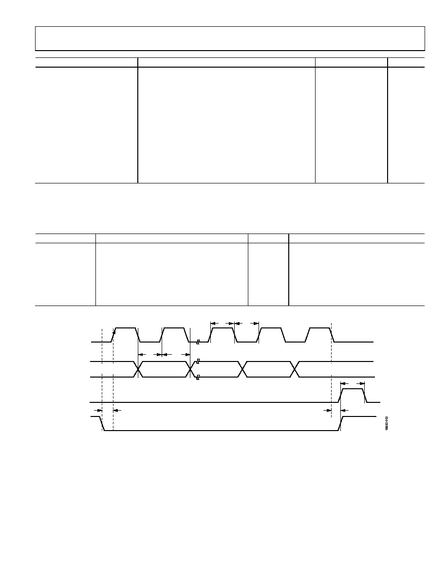 Data Sheet ADRF6807 Rev. B | Page 5 of 36 Parameter Test Conditions/Comments Min Typ Max Unit POWER SUPPLIES VCC1, VCC2, VCCLO, VCCBB, VCCRF pins Voltage Range (3.3 V) VCC1, VCC2, VCCLO 3.135 3.3 3.465 V Voltage Range (5 V) VCCBB, VCCRF 4.75 5 5.25 V Supply Current (3.3 V) (LPEN = 0) Normal Rx mode 170 mA Rx mode with LO buffer enabled 227 mA Supply Current (5 V) (LPEN = 0) Normal Rx mode 86 mA Rx mode with LO buffer enabled 86 mA Supply Current (3.3 V) (LPEN = 1) Normal Rx mode 166 mA Rx mode with LO buffer enabled 214 mA Supply Current (5 V) (LPEN = 1) Normal Rx mode 76 mA Rx mode with LO buffer enabled 76 mA Supply Current (5 V) Power-down mode 10 mA Supply Current (3.3 V) Power-down mode 15 mA TIMING CHARACTERISTICS VS1 (VVCCBB and VVCCRF) = 5 V, and VS2 (VVCC1, VVCC2, and VVCCLO) = 3.3 V. Table 2. Parameter Limit at TMIN to TMAX Unit Test Conditions/Comments t1 20 ns min LE setup time t2 10 ns min DATA to CLK setup time t3 10 ns min DATA to CLK hold time t4 25 ns min CLK high duration t5 25 ns min CLK low duration t6 10 ns min CLK to LE setup time t7 20 ns min LE pulse width CLK DATA LE LE DB23 (MSB) DB22 DB2 (CONTROL BIT C3) DB1 (CONTROL BIT C2) DB0 (LSB) (CONTROL BIT C1) t1 t2 t3 t7 t6 t4 t5 Figure 2. Timing Diagram |
|
Enlace URL |
| ¿ALLDATASHEET es útil para Ud.? [ DONATE ] |
Todo acerca de Alldatasheet | Publicidad | Contáctenos | Política de Privacidad | Enlace a la hoja de datos | Intercambio de Enlaces | Lista de Fabricantes All Rights Reserved©Alldatasheet.com |
| Russian : Alldatasheetru.com | Korean : Alldatasheet.co.kr | Spanish : Alldatasheet.es | French : Alldatasheet.fr | Italian : Alldatasheetit.com Portuguese : Alldatasheetpt.com | Polish : Alldatasheet.pl | Vietnamese : Alldatasheet.vn Indian : Alldatasheet.in | Mexican : Alldatasheet.com.mx | British : Alldatasheet.co.uk | New Zealand : Alldatasheet.co.nz |
|
Family Site : ic2ic.com |
icmetro.com |
 Mexican ▼
 English
 Chinese
 German
 Japanese
 Russian
 Korean
 Spanish
 French
 Italian
 Portuguese
 Polish
 Vietnamese
 Indian
 Mexican
 British
 New Zealand


