|
Motor de Búsqueda de Datasheet de Componentes Electrónicos |
|
|
Motor de Búsqueda de Datasheet de Componentes Electrónicos |
|
AD7841ASZ Datasheet(PDF) 9 Page - Analog Devices |
|
|
|||||||||||||||||||||||||||||
AD7841ASZ Datasheet(HTML) 9 Page - Analog Devices |
|
|
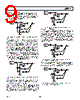
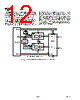
9 / 13 page  AD7841 –9– Power-On with CLR Low The output stage of the AD7841 has been designed to allow output stability during power-on. If CLR is kept low during power-on, then just after power is applied to the AD7841, the situation is as depicted in Figure 5. G1, G4 and G6 are open while G2, G3 and G5 are closed. G1 G2 G4 G3 G6 G5 DUTGND VOUT R R 14k DAC Figure 5. Output Stage with VDD < 7 V or VSS > –3 V; CLR Low VOUT is kept within a few hundred millivolts of DUTGND via G5 and a 14 k Ω resistor. This thin-film resistor is connected in parallel with the gain resistors of the output amplifier. The output amplifier is connected as a unity gain buffer via G3, and the DUTGND voltage is applied to the buffer input via G2. The amplifier’s output is thus at the same voltage as the DUTGND pin. The output stage remains configured as in Figure 5 until the voltage at VDD exceeds 7 V and VSS is more negative than –3 V. By now the output amplifier has enough headroom to handle signals at its input and has also had time to settle. The internal power-on circuitry opens G3 and G5 and closes G4 and G6. This situation is shown in Figure 6. Now the output ampli- fier is configured in its noise gain configuration via G4 and G6. The DUTGND voltage is still connected to the noninverting input via G2 and this voltage appears at VOUT. G1 G2 G4 G3 G6 G5 DUTGND VOUT R R 14k DAC Figure 6. Output Stage with VDD > 7 V and VSS < –3 V; CLR Low VOUT has been disconnected from the DUTGND pin by the opening of G5, but will track the voltage present at DUTGND via the configuration shown in Figure 6. When CLR is taken back high, the output stage is configured as shown in Figure 7. The internal control logic closes G1 and opens G2. The output amr})fier is connected in a noninverting gain-of-two configuration. The voltage that appears on the VOUT pins is determined by the data present in the DAC registers. G1 G2 G4 G3 G6 G5 DUTGND VOUT R R 14k DAC Figure 7. Output Stage After CLR Is Taken High Power-On with CLR High If CLR is high on the application of power to the device, the output stages of the AD7841 are configured as in Figure 8 while VDD is less than 7 V and VSS is more positive than –3 V. G1 is closed and G2 is open, thereby connecting the output of the DAC to the input of its output amplifier. G3 and G5 are closed while G4 and G6 are open, thus connecting the output amplifier as a unity gain buffer. VOUT is connected to DUTGND via G5 through a 14 k Ω resistor until V DD exceeds 7 V and VSS is more negative than –3 V. G1 G2 G4 G3 G6 G5 DUTGND VOUT R R 14k DAC Figure 8. Output Stage Powering Up with CLR High While VDD < 7 V or VSS > –3 V When the difference between the supply voltages reaches 10 V, the internal power-on circuitry opens G3 and G5 and closes G4 and G6 configuring the output stage as shown in Figure 9. G1 G2 G4 G3 G6 G5 DUTGND VOUT R R 14k DAC Figure 9. Output Stage Powering Up with CLR High When VDD > 7 V and VSS < –3 V REV. B |
|
|
Enlace URL |
| ¿ALLDATASHEET es útil para Ud.? [ DONATE ] |
Todo acerca de Alldatasheet | Publicidad | Contáctenos | Política de Privacidad | Enlace a la hoja de datos | Intercambio de Enlaces | Lista de Fabricantes All Rights Reserved©Alldatasheet.com |
| Russian : Alldatasheetru.com | Korean : Alldatasheet.co.kr | Spanish : Alldatasheet.es | French : Alldatasheet.fr | Italian : Alldatasheetit.com Portuguese : Alldatasheetpt.com | Polish : Alldatasheet.pl | Vietnamese : Alldatasheet.vn Indian : Alldatasheet.in | Mexican : Alldatasheet.com.mx | British : Alldatasheet.co.uk | New Zealand : Alldatasheet.co.nz |
|
Family Site : ic2ic.com |
icmetro.com |
 Mexican ▼
 English
 Chinese
 German
 Japanese
 Russian
 Korean
 Spanish
 French
 Italian
 Portuguese
 Polish
 Vietnamese
 Indian
 Mexican
 British
 New Zealand