|
Motor de Búsqueda de Datasheet de Componentes Electrónicos |
|
|
Motor de Búsqueda de Datasheet de Componentes Electrónicos |
|
AD7841ASZ Datasheet(PDF) 12 Page - Analog Devices |
|
|
|||||||||||||||||||||||||||||
AD7841ASZ Datasheet(HTML) 12 Page - Analog Devices |
|
|
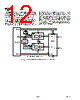
12 / 13 page  AD7841 –12– GND VDD 8/10-BIT DAC GND VDD 8/10-BIT DAC LOGIC LEVEL SHIFT +5V 5V SCLK D IN FSIN/CS SCLK D IN FSIN/CS 0V TO +5V 0V TO 5V VREF(+)AB A0, A1, A2 VOUTA VOUTA VOUTB VOUTB VREF( )AB AD7841* GND DATA BUS ADDR DECODER ADDR BUS SDATA SCLK DATA BUS CONTROLLER *ADDITIONAL PINS OMITTED FOR CLARITY Figure 13. Programmable Reference Generation for the AD7841 The AD8803 has an output voltage range of GND to VDD (0 V to 5 V). To trim the VREF(+) input, the appropriate trim range on the AD8803 DAC can be set using the VREFL and VREFH pins allowing 8 bits of resolution between the two points. This will allow the VREF(+) pin to be adjusted to remove gain errors. To trim the VREF(–) voltage, some method of providing a trim voltage in the required negative voltage range is required. Neither the AD7804 or the AD8803 can provide this range in normal operation as their output range is 0 V to 5 V. There are two methods of producing this negative voltage. One method is to provide a positive output voltage and then to level shift that ana- log voltage to the required negative range. Alternatively these DACs can be operated with supplies of 0 V and –5 V, with the VDD pin connected to 0 V and the GND pin connected to –5 V. Now these can be used to provide the negative reference volt- ages for the VREF(–) inputs on the AD7841. However, the digital signals driving the DACs need to be level-shifted from the 0 V to +5 V range to the –5 V to 0 V range. Figure 13 shows a typical application circuit to provide programmable reference capabilities for the AD7841. REV. B |
|
|
Enlace URL |
| ¿ALLDATASHEET es útil para Ud.? [ DONATE ] |
Todo acerca de Alldatasheet | Publicidad | Contáctenos | Política de Privacidad | Enlace a la hoja de datos | Intercambio de Enlaces | Lista de Fabricantes All Rights Reserved©Alldatasheet.com |
| Russian : Alldatasheetru.com | Korean : Alldatasheet.co.kr | Spanish : Alldatasheet.es | French : Alldatasheet.fr | Italian : Alldatasheetit.com Portuguese : Alldatasheetpt.com | Polish : Alldatasheet.pl | Vietnamese : Alldatasheet.vn Indian : Alldatasheet.in | Mexican : Alldatasheet.com.mx | British : Alldatasheet.co.uk | New Zealand : Alldatasheet.co.nz |
|
Family Site : ic2ic.com |
icmetro.com |
 Mexican ▼
 English
 Chinese
 German
 Japanese
 Russian
 Korean
 Spanish
 French
 Italian
 Portuguese
 Polish
 Vietnamese
 Indian
 Mexican
 British
 New Zealand