 |
Motor de Búsqueda de Datasheet de Componentes Electrónicos |
|
|
Motor de Búsqueda de Datasheet de Componentes Electrónicos |
|
AX2000 Datasheet(PDF) 21 Page - Microsemi Corporation |
|
|
|||||||||||||||||||||||||||||
AX2000 Datasheet(HTML) 21 Page - Microsemi Corporation |
|
|
21 / 262 page 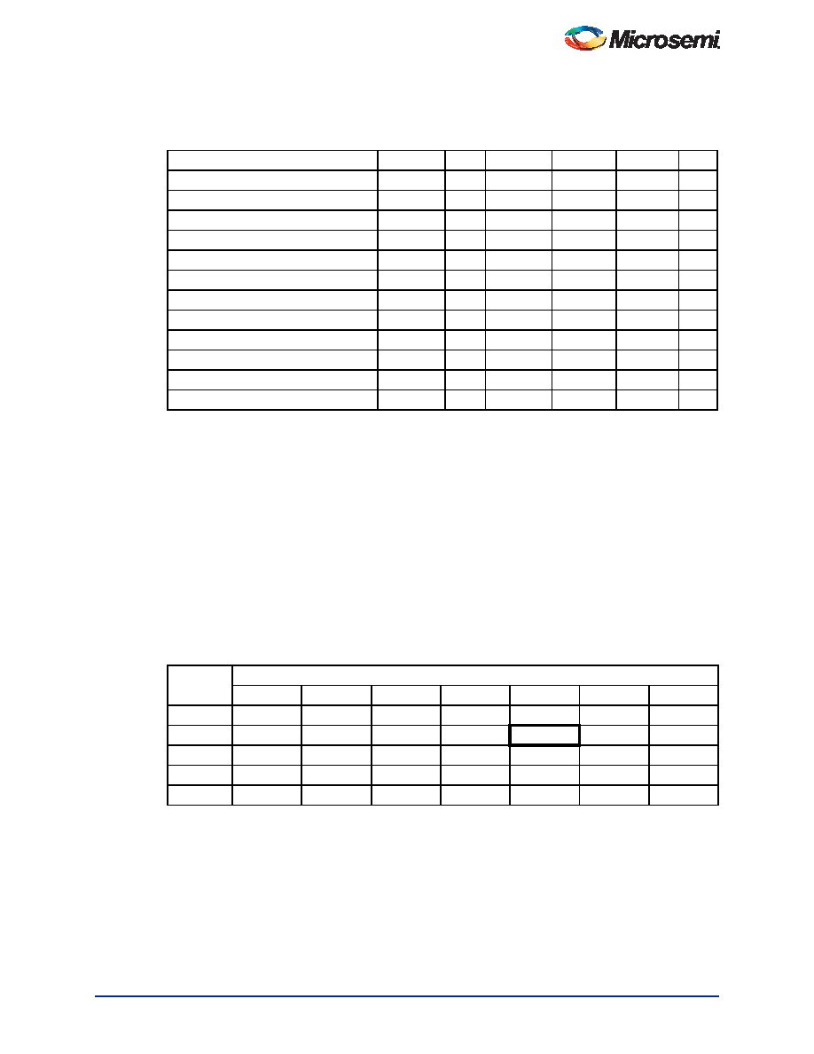 Axcelerator Family FPGAs Re vi s i on 18 2-7 The maximum power dissipation allowed for Military temperature and Mil-Std 883B devices is specified as a function of θjc. Timing Characteristics Axcelerator devices are manufactured in a CMOS process, therefore, device performance varies according to temperature, voltage, and process variations. Minimum timing parameters reflect maximum operating voltage, minimum operating temperature, and best-case processing. Maximum timing parameters reflect minimum operating voltage, maximum operating temperature, and worst-case processing. The derating factors shown in Table 2-7 should be applied to all timing data contained within this datasheet. All timing numbers listed in this datasheet represent sample timing characteristics of Axcelerator devices. Actual timing delay values are design-specific and can be derived from the Timer tool in Microsemi’s Designer software after place-and-route. Table 2-6 • Package Thermal Characteristics Package Type Pin Count θ jc θ ja Still Air θ ja 1.0m/s θ ja 2.5m/s Units Chip Scale Package (CSP) 180 N/A 57.8 51.0 50 °C/W Plastic Quad Flat Pack (PQFP) 208 8.0 26 23.5 20.9 °C/W Plastic Ball Grid Array (PBGA) 729 2.2 13.7 10.6 9.6 °C/W Fine Pitch Ball Grid Array (FBGA) 256 3.0 26.6 22.8 21.5 °C/W Fine Pitch Ball Grid Array (FBGA) 324 3.0 25.8 22.1 20.9 °C/W Fine Pitch Ball Grid Array (FBGA) 484 3.2 20.5 17.0 15.9 °C/W Fine Pitch Ball Grid Array (FBGA) 676 3.2 16.4 13.0 12.0 °C/W Fine Pitch Ball Grid Array (FBGA) 896 2.4 13.6 10.4 9.4 °C/W Fine Pitch Ball Grid Array (FBGA) 1152 1.8 12.0 8.9 7.9 °C/W Ceramic Quad Flat Pack (CQFP)1 208 2.0 22 19.8 18.0 °C/W Ceramic Quad Flat Pack (CQFP)1 352 2.0 17.9 16.1 14.7 °C/W Ceramic Column Grid Array (CCGA)2 624 6.5 8.9 8.5 8 °C/W Notes: 1. θjc for the 208-pin and 352-pin CQFP refers to the thermal resistance between the junction and the bottom of the package. 2. θjc for the 624-pin CCGA refers to the thermal resistance between the junction and the top surface of the package. Thermal resistance from junction to board ( θ jb) for CCGA 624 package is 3.4°C/W. Table 2-7 • Temperature and Voltage Timing Derating Factors (Normalized to Worst-Case Commercial, TJ = 70°C, VCCA = 1.425V) VCCA Junction Temperature –55°C –40°C 0°C 25°C 70°C 85°C 125°C 1.4 V 0.83 0.86 0.91 0.96 1.02 1.05 1.15 1.425 V 0.82 0.84 0.90 0.94 1.00 1.04 1.13 1.5 V 0.78 0.80 0.85 0.89 0.95 0.98 1.07 1.575 V 0.74 0.76 0.81 0.85 0.90 0.94 1.02 1.6 V 0.73 0.75 0.80 0.84 0.89 0.92 1.01 Notes: 1. The user can set the junction temperature in Designer software to be any integer value in the range of – 55 °C to 175°C. 2. The user can set the core voltage in Designer software to be any value between 1.4V and 1.6V. |
|
Enlace URL |
| ¿ALLDATASHEET es útil para Ud.? [ DONATE ] |
Todo acerca de Alldatasheet | Publicidad | Contáctenos | Política de Privacidad | Enlace a la hoja de datos | Intercambio de Enlaces | Lista de Fabricantes All Rights Reserved©Alldatasheet.com |
| Russian : Alldatasheetru.com | Korean : Alldatasheet.co.kr | Spanish : Alldatasheet.es | French : Alldatasheet.fr | Italian : Alldatasheetit.com Portuguese : Alldatasheetpt.com | Polish : Alldatasheet.pl | Vietnamese : Alldatasheet.vn Indian : Alldatasheet.in | Mexican : Alldatasheet.com.mx | British : Alldatasheet.co.uk | New Zealand : Alldatasheet.co.nz |
|
Family Site : ic2ic.com |
icmetro.com |
 Mexican ▼
 English
 Chinese
 German
 Japanese
 Russian
 Korean
 Spanish
 French
 Italian
 Portuguese
 Polish
 Vietnamese
 Indian
 Mexican
 British
 New Zealand


