 |
Motor de Búsqueda de Datasheet de Componentes Electrónicos |
|
|
Motor de Búsqueda de Datasheet de Componentes Electrónicos |
|
M24C08-R Datasheet(PDF) 8 Page - STMicroelectronics |
|
|
|||||||||||||||||||||||||||||
M24C08-R Datasheet(HTML) 8 Page - STMicroelectronics |
|
|
8 / 38 page 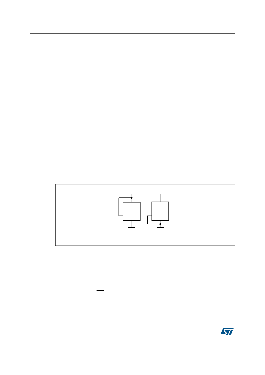 Signal description M24C08-W M24C08-R M24C08-F 8/38 DocID023924 Rev 4 2 Signal description 2.1 Serial Clock (SCL) The signal applied on the SCL input is used to strobe the data available on SDA(in) and to output the data on SDA(out). 2.2 Serial Data (SDA) SDA is an input/output used to transfer data in or data out of the device. SDA(out) is an open drain output that may be wire-OR’ed with other open drain or open collector signals on the bus. A pull-up resistor must be connected from Serial Data (SDA) to VCC (Figure 12 indicates how to calculate the value of the pull-up resistor). 2.3 Chip Enable (E2) This input signal is used to set the value that is to be looked for on the bit b3 of the device select code. This input must be tied to VCC or VSS, to establish the device select code as shown in Figure 4. When not connected (left floating), this input is read as low (0). Figure 4. Chip enable inputs connection 2.4 Write Control (WC) This input signal is useful for protecting the entire contents of the memory from inadvertent write operations. Write operations are disabled to the entire memory array when Write Control (WC) is driven high. Write operations are enabled when Write Control (WC) is either driven low or left floating. When Write Control (WC) is driven high, device select and address bytes are acknowledged, Data bytes are not acknowledged. Ai12806 VCC M24xxx VSS Ei VCC M24xxx VSS Ei |
|
Enlace URL |
| ¿ALLDATASHEET es útil para Ud.? [ DONATE ] |
Todo acerca de Alldatasheet | Publicidad | Contáctenos | Política de Privacidad | Enlace a la hoja de datos | Intercambio de Enlaces | Lista de Fabricantes All Rights Reserved©Alldatasheet.com |
| Russian : Alldatasheetru.com | Korean : Alldatasheet.co.kr | Spanish : Alldatasheet.es | French : Alldatasheet.fr | Italian : Alldatasheetit.com Portuguese : Alldatasheetpt.com | Polish : Alldatasheet.pl | Vietnamese : Alldatasheet.vn Indian : Alldatasheet.in | Mexican : Alldatasheet.com.mx | British : Alldatasheet.co.uk | New Zealand : Alldatasheet.co.nz |
|
Family Site : ic2ic.com |
icmetro.com |
 Mexican ▼
 English
 Chinese
 German
 Japanese
 Russian
 Korean
 Spanish
 French
 Italian
 Portuguese
 Polish
 Vietnamese
 Indian
 Mexican
 British
 New Zealand


