|
Motor de Búsqueda de Datasheet de Componentes Electrónicos |
|
|
Motor de Búsqueda de Datasheet de Componentes Electrónicos |
|
LTC485CS8 Datasheet(PDF) 8 Page - Linear Technology |
|
|
|||||||||||||||||||||||||||||
LTC485CS8 Datasheet(HTML) 8 Page - Linear Technology |
|
|
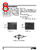
8 / 12 page  8 LTC485 APPLICATIO S I FOR ATIO The LTC485 output stage will maintain a high impedance state until the breakdown of the N-channel or P-channel is reached when going positive or negative respectively. The output will be clamped to either VCC or ground by a Zener voltage plus a Schottky diode drop, but this voltage is way beyond the RS485 operating range. This clamp protects the MOS gates from ESD voltages well over 2000V. Because the ESD injected current in the N-well or substrate consists of majority carriers, latchup is prevented by careful layout techniques. Propagation Delay Many digital encoding schemes are dependent upon the difference in the propagation delay times of the driver and the receiver. Using the test circuit of Figure 13, Figures 11 and 12 show the typical LTC485 receiver propagation delay. The receiver delay times are: tPLH – tPHL = 9ns Typ, VCC = 5V The driver skew times are: Skew = 5ns Typ, VCC = 5V 10ns Max, VCC = 5V, TA = –40°C to 85°C Figure 11. Receiver tPHL Figure 12. Receiver tPLH D R RECEIVER OUT R 100 Ω 100pF 100pF TTL IN tr, tf < 6ns BR LTC485 • F13 Figure 13. Receiver Propagation Delay Test Circuit LTC485 • F11 RO B A DRIVER OUTPUTS RECEIVER OUTPUT A B RO RECEIVER OUTPUT DRIVER OUTPUTS LTC485 • F12 |
|
|
Enlace URL |
| ¿ALLDATASHEET es útil para Ud.? [ DONATE ] |
Todo acerca de Alldatasheet | Publicidad | Contáctenos | Política de Privacidad | Enlace a la hoja de datos | Intercambio de Enlaces | Lista de Fabricantes All Rights Reserved©Alldatasheet.com |
| Russian : Alldatasheetru.com | Korean : Alldatasheet.co.kr | Spanish : Alldatasheet.es | French : Alldatasheet.fr | Italian : Alldatasheetit.com Portuguese : Alldatasheetpt.com | Polish : Alldatasheet.pl | Vietnamese : Alldatasheet.vn Indian : Alldatasheet.in | Mexican : Alldatasheet.com.mx | British : Alldatasheet.co.uk | New Zealand : Alldatasheet.co.nz |
|
Family Site : ic2ic.com |
icmetro.com |
 Mexican ▼
 English
 Chinese
 German
 Japanese
 Russian
 Korean
 Spanish
 French
 Italian
 Portuguese
 Polish
 Vietnamese
 Indian
 Mexican
 British
 New Zealand