|
Motor de Búsqueda de Datasheet de Componentes Electrónicos |
|
|
Motor de Búsqueda de Datasheet de Componentes Electrónicos |
|
SP6128A Datasheet(PDF) 3 Page - Exar Corporation |
|
|
|||||||||||||||||||||||||||||
SP6128A Datasheet(HTML) 3 Page - Exar Corporation |
|
|
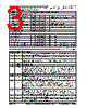
3 / 10 page  3 Rev. 08/19/05 SP6128A Low Voltage, Synchronous Step Down PWM Controller © Copyright 2005 Sipex Corporation PIN DESCRIPTION PIN N0. PIN NAME DESCRIPTION 1 GL High current driver output for the low side MOSFET switch. It is always low if GH is high. GL swings from PGND to PVCC. 2 PVCC Positive input supply for the low side gate driver. It's recommended to tie the PVCC to the VCC pin. 3 VCC Positive input supply for the logic circuitry. Properly bypass this pin to GND with a low ESL/ ESR ceramic capacitor or RC filter. 4 PGND Power ground pin. 5 GND Signal ground pin. 6 COMP Output of the Error Amplifier. It is internally connected to the inverting input of the PWM comparator. A lead-lag network is typically connected to the COMP pin to compensate the feedback loop in order to optimize the dynamic performance of the voltage mode control loop. Sleep mode can be invoked by pulling the COMP pin below 0.3V with an external open-drain or open-collector transistor. An internal 5µA pull-up ensures start-up. 7, 8, 9 NC No connect. 10 VFB Feedback Voltage Pin. It is the inverting input of the Error Amplifier and serves as the output voltage feedback point for the Buck converter. The output voltage is sensed and can be adjusted through an external resistor divider. 11 ISET Overcurrent program pin. A resistor programs the overcurrent threshold. The overcurrent comparator sets the fault latch and terminates gate pulses when VISET > VSWN and the high side MOSFET is turned on. This prevents excessive power dissipation in the external power MOSFETs during an overload condition. An internal delay circuit prevents false shutdowns that might otherwise occur during very short, mild overload conditions,due to load transients. 12 SWN Lower supply rail for the GH high-side gate driver. It also connects to the Current Limit comparator. Connect this pin to the switching node at the junction between the two external power MOSFET transistors. This pin monitors the voltage drop across the RDS(ON) of the high side N-channel MOSFET while it is conducting. 13 GH High current driver output for the high side MOSFET switch. It is always low if GL is high or during a fault. GH swings from SWN to BST. 14 BST High side driver supply pin. Connect BST to the external boost diode and capacitor as shown in the application schematic on page 1. ELECTRICAL CHARACTERISTICS Unless otherwise specified: -40°C < TA < 85°C, 3.0V < PVCC = VCC < 5.5V, CCOMP = 22nF, CGH = CGL = 3.3nF, VFB = 0.8V, SWN = GND = 0V, typical value for design guideline only. PARAMETER MIN TYP MAX UNITS CONDITIONS SOFT START, SHUTDOWN, UVLO Internal Soft Start Slew Rate 0.1 0.3 0.6 V/ms COMP pin, on transition from shutdown COMP Discharge Current 183 µA COMP = 0.5V, Fault Initiated COMP Clamp Voltage 0.55 0.65 0.75 V VFB = 0.9V COMP Clamp Current 10 30 65 µA COMP = 0.5V, VFB = 0.9V Shutdown Threshold Voltage 0.29 0.34 0.39 V Measured at COMP Pin Shutdown Input Pull-up Current 2 5 10 µA COMP = 0.2V, Measured at COMP pin VCC Start Threshold 2.63 2.8 2.95 V VCC Stop Threshold 2.47 2.7 2.9 V GATE DRIVERS GH Rise Time 60 110 ns PVCC > 4.5V GH Fall Time 60 110 ns PVCC > 4.5V GL Rise Time 60 110 ns PVCC > 4.5V GL Fall Time 60 110 ns PVCC > 4.5V GH to GL Non-Overlap Time 0 100 140 ns PVCC > 4.5V, measured at 2volt threshold GL to GH Non-Overlap Time 0 100 140 ns PVCC > 4.5V, measured at 2volt threshold |
|
|
Enlace URL |
| ¿ALLDATASHEET es útil para Ud.? [ DONATE ] |
Todo acerca de Alldatasheet | Publicidad | Contáctenos | Política de Privacidad | Enlace a la hoja de datos | Intercambio de Enlaces | Lista de Fabricantes All Rights Reserved©Alldatasheet.com |
| Russian : Alldatasheetru.com | Korean : Alldatasheet.co.kr | Spanish : Alldatasheet.es | French : Alldatasheet.fr | Italian : Alldatasheetit.com Portuguese : Alldatasheetpt.com | Polish : Alldatasheet.pl | Vietnamese : Alldatasheet.vn Indian : Alldatasheet.in | Mexican : Alldatasheet.com.mx | British : Alldatasheet.co.uk | New Zealand : Alldatasheet.co.nz |
|
Family Site : ic2ic.com |
icmetro.com |
 Mexican ▼
 English
 Chinese
 German
 Japanese
 Russian
 Korean
 Spanish
 French
 Italian
 Portuguese
 Polish
 Vietnamese
 Indian
 Mexican
 British
 New Zealand