|
Motor de Búsqueda de Datasheet de Componentes Electrónicos |
|
|
Motor de Búsqueda de Datasheet de Componentes Electrónicos |
|
LM2716 Datasheet(PDF) 11 Page - National Semiconductor (TI) |
|
|
|
|||||||||||||||||||||||||||||
LM2716 Datasheet(HTML) 11 Page - National Semiconductor (TI) |
|
|
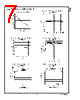
11 / 17 page  Boost Operation CONTINUOUS CONDUCTION MODE The LM2716 contains a current-mode, PWM boost regulator. A boost regulator steps the input voltage up to a higher output voltage. In continuous conduction mode (when the inductor current never reaches zero at steady state), the boost regulator operates in two cycles. In the first cycle of operation, shown in Figure 1 (a), the transistor is closed and the diode is reverse biased. Energy is collected in the inductor and the load current is supplied by C OUT. The second cycle is shown in Figure 1 (b). During this cycle, the transistor is open and the diode is forward biased. The energy stored in the inductor is transferred to the load and output capacitor. The ratio of these two cycles determines the output voltage. The output voltage is defined approximately as: where D is the duty cycle of the switch, D and D' will be required for design calculations. SETTING THE OUTPUT VOLTAGE The output voltage is set using the feedback pin and a resistor divider connected to the output as shown in Figure 3. The feedback pin voltage is 1.26V, so the ratio of the feed- back resistors sets the output voltage according to the fol- lowing equation: INTRODUCTION TO COMPENSATION 20071202 FIGURE 1. Simplified Boost Converter Diagram (a) First Cycle of Operation (b) Second Cycle Of Operation 20071205 FIGURE 2. (a) Inductor current. (b) Diode current. www.national.com 11 |
|
|
Enlace URL |
| ¿ALLDATASHEET es útil para Ud.? [ DONATE ] |
Todo acerca de Alldatasheet | Publicidad | Contáctenos | Política de Privacidad | Enlace a la hoja de datos | Intercambio de Enlaces | Lista de Fabricantes All Rights Reserved©Alldatasheet.com |
| Russian : Alldatasheetru.com | Korean : Alldatasheet.co.kr | Spanish : Alldatasheet.es | French : Alldatasheet.fr | Italian : Alldatasheetit.com Portuguese : Alldatasheetpt.com | Polish : Alldatasheet.pl | Vietnamese : Alldatasheet.vn Indian : Alldatasheet.in | Mexican : Alldatasheet.com.mx | British : Alldatasheet.co.uk | New Zealand : Alldatasheet.co.nz |
|
Family Site : ic2ic.com |
icmetro.com |
 Mexican ▼
 English
 Chinese
 German
 Japanese
 Russian
 Korean
 Spanish
 French
 Italian
 Portuguese
 Polish
 Vietnamese
 Indian
 Mexican
 British
 New Zealand