 |
Motor de Búsqueda de Datasheet de Componentes Electrónicos |
|
|
Motor de Búsqueda de Datasheet de Componentes Electrónicos |
|
The question interval is too short.
Please try again in a few seconds.

Hello, Please ask a question about SL28647CLC Datasheet
# Example questions:
➢ Several control registers (e.g., byte 4, byte 5) have 'stp_ctrl' bits. what do these bits control, and what is the effect of setting them to '0' versus '1'?
➢ G. byte 7, byte 9, byte 10). what does 'slew rate' refer to in this context and what is indicated by setting the 'bit0' of those registers to '0' versus '1'?
➢ What is the purpose of bits 0-3 in byte 8, and how do they relate to identifying the device?
| Part No. | SL28647CLC |
| Manufacturer | SILABS |
| Size | 275 Kbytes |
| Pages | 27 pages |
| Description | Clock Generator for Intel짰CK505 |


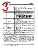
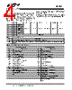


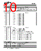


This document details the control registers for a chip (likely a clock/timing or interface chip) designated "SL28647". Here's a summary of the key information:
Overall Function:
️· The chip appears to be a configurable clock generator/distribution/interface, offering significant control over output signals (PCI, PCIF, SRC, REF clocks, etc.).
️· It provides options for controlling signal slew rates, drive modes (driven/tri-state), and synchronization using various control bits and signals (PCI_STP, CPU_STP, PD, FSC, FSB, FSA).
️· The registers allow configuration of clock outputs, power-down behavior, and potentially testing/debugging modes.
Key Features & Registers:
️· Registers 0-7 (Bytes 0-7): These are the primary control registers. They control various output signals (PCI, PCIF, SRC, REF) and their behaviors (slew rate, drive mode, stop control). They also contain configuration bits for testing and power-up settings (FSC, FSB, FSA).
️· Byte 7: Contains test selection bits and reflects the values of external pins (FSC, FSB, FSA) at power-up.
️· Byte 8: Contains Vendor ID and Revision Code information.
️· Byte 9 & 10: These registers provide further control over slew rates for specific clock outputs (48M, PCIF0).
Important Control Concepts:
️· Drive Modes: The chip can switch outputs between being actively driven and a high-impedance (tri-state) mode, offering flexibility for system-level control.
️· Stop Control: The chip allows outputs to be stopped or resumed synchronously, preventing signal glitches.
️· Slew Rate Control: Adjusting the slew rate of signals can reduce electromagnetic interference (EMI).
️· Power-Down Control: The chip can drive or tri-state outputs during power-down, allowing for controlled shutdown behavior.
️· External Pin Reflection: The value of certain external pins (FSC, FSB, FSA) at power-up are reflected within the chip for configuration.
How to Interpret the Tables:
️· Bit: Indicates the specific bit within the byte register.
️· @Pup: Represents the power-up default value of the bit (likely '1' for high, '0' for low).
️· Name: The symbolic name of the control bit.
️· Description: A detailed explanation of the bit's function.
In summary, this document provides the necessary information to program and control the SL28647 chip, allowing for precise configuration of its clock and interface outputs.
Overall Function:
️· The chip appears to be a configurable clock generator/distribution/interface, offering significant control over output signals (PCI, PCIF, SRC, REF clocks, etc.).
️· It provides options for controlling signal slew rates, drive modes (driven/tri-state), and synchronization using various control bits and signals (PCI_STP, CPU_STP, PD, FSC, FSB, FSA).
️· The registers allow configuration of clock outputs, power-down behavior, and potentially testing/debugging modes.
Key Features & Registers:
️· Registers 0-7 (Bytes 0-7): These are the primary control registers. They control various output signals (PCI, PCIF, SRC, REF) and their behaviors (slew rate, drive mode, stop control). They also contain configuration bits for testing and power-up settings (FSC, FSB, FSA).
️· Byte 7: Contains test selection bits and reflects the values of external pins (FSC, FSB, FSA) at power-up.
️· Byte 8: Contains Vendor ID and Revision Code information.
️· Byte 9 & 10: These registers provide further control over slew rates for specific clock outputs (48M, PCIF0).
Important Control Concepts:
️· Drive Modes: The chip can switch outputs between being actively driven and a high-impedance (tri-state) mode, offering flexibility for system-level control.
️· Stop Control: The chip allows outputs to be stopped or resumed synchronously, preventing signal glitches.
️· Slew Rate Control: Adjusting the slew rate of signals can reduce electromagnetic interference (EMI).
️· Power-Down Control: The chip can drive or tri-state outputs during power-down, allowing for controlled shutdown behavior.
️· External Pin Reflection: The value of certain external pins (FSC, FSB, FSA) at power-up are reflected within the chip for configuration.
How to Interpret the Tables:
️· Bit: Indicates the specific bit within the byte register.
️· @Pup: Represents the power-up default value of the bit (likely '1' for high, '0' for low).
️· Name: The symbolic name of the control bit.
️· Description: A detailed explanation of the bit's function.
In summary, this document provides the necessary information to program and control the SL28647 chip, allowing for precise configuration of its clock and interface outputs.
| Part No. | SL28647CLC |
| Manufacturer | SILABS |
| Size | 275 Kbytes |
| Pages | 27 pages |
| Description | Clock Generator for Intel짰CK505 |
| ¿ALLDATASHEET es útil para Ud.? [ DONATE ] |
Todo acerca de Alldatasheet | Publicidad | Contáctenos | Política de Privacidad | Enlace a la hoja de datos | Intercambio de Enlaces | Lista de Fabricantes All Rights Reserved©Alldatasheet.com |
| Russian : Alldatasheetru.com | Korean : Alldatasheet.co.kr | Spanish : Alldatasheet.es | French : Alldatasheet.fr | Italian : Alldatasheetit.com Portuguese : Alldatasheetpt.com | Polish : Alldatasheet.pl | Vietnamese : Alldatasheet.vn Indian : Alldatasheet.in | Mexican : Alldatasheet.com.mx | British : Alldatasheet.co.uk | New Zealand : Alldatasheet.co.nz |
|
Family Site : ic2ic.com |
icmetro.com |
 Mexican ▼
  English
 Chinese
 German
 Japanese
 Russian
 Korean
 Spanish
 French
 Italian
 Portuguese
 Polish
 Vietnamese
 Indian
 British
 New Zealand