|
Motor de Búsqueda de Datasheet de Componentes Electrónicos |
|
|
Motor de Búsqueda de Datasheet de Componentes Electrónicos |
|
SL28647CLC Datasheet(PDF) 2 Page - Silicon Laboratories |
|
|
|||||||||||||||||||||||||||||
SL28647CLC Datasheet(HTML) 2 Page - Silicon Laboratories |
|
|
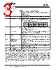
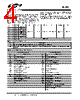
2 / 27 page  SL28647 .......................Document #: 001-05103 Rev *B Page 2 of 27 Pin Description Pin No. Name Type Description 1, 49, 54, 65 VDD_SRC PWR 3.3V power supply for outputs. 2, 3, 52, 53, 55, 56, 58, 59, 60, 61, 63, 64, 66, 67, 69, 70 SRCT/C[2:9] O, DIF 100-MHz Differential serial reference clocks. 4, 68 VSS_SRC GND Ground for outputs. 5, 6 CPUT2_ITP/SRCT10, CPUC2_ITP/SRCC10 O, DIF Selectable differential CPU or SRC clock output. ITP_SEL = 0 @ pin 39 assertion = SRC10 ITP_SEL = 1 @ pin 39 assertion = CPU2 7 VDDA PWR 3.3V power supply for PLL. 8 VSSA GND Ground for PLL. 9 NC NC No Connect Pin 10, 11 CPUC1_MCH, CPUT1_MCH O, DIF Differential CPU clock output to MCH 12 VDD_CPU PWR 3.3V power supply for outputs. 13, 14 CPU[T/C]0 O, DIF Differential CPU clock output 15 VSS_CPU GND Ground for outputs. 16 SCLK I SMBus-compatible SCLOCK. 17 SDATA I/O, OD SMBus-compatible SDATA. 18 VDD_REF PWR 3.3V power supply for outputs. 19 XOUT O, SE 14.318-MHz crystal output. 20 XIN I 14.318-MHz crystal input. 21 VSS_REF GND Ground for outputs. 22 REF1 O Fixed 14.318-MHz clock output. 23 REF0/FSC_TESTSEL I/O Fixed 14.318 clock output/3.3V-tolerant input for CPU frequency selection/Selects test mode if pulled to VIMFS_C when pin 39 is asserted LOW. Refer to DC Electrical Specifications table for VILFS_C,VIMFS_C,VIHFS_C specifi- cations. 24 CPU_STP# I 3.3V LVTTL input for CPU_STP# active LOW During direct clock off to M1 mode transition, a serial load of BSEL data is driven on this pin and sampled on the rising edge of PCI_STP#. See Figure 14.for more information. 25 PCI_STP# I 3.3V LVTTL input for PCI_STP# active LOW During direct clock off to M1 mode transition, a serial load of BSEL data is driven on CPU_STP# and sampled on the rising edge of this pin. See Figure 14. for more information. 26, 28, 29, 38, 46, 57, 62, 71, 72 CLKREQ[1:9]# I 3.3V LVTTL input for enabling assigned SRC clock (active LOW). 27 PCI1 I/O, SE 33MHz clock output 30, 36 VDD_PCI PWR 3.3V power supply for outputs. 31, 35 VSS_PCI GND Ground for outputs. |
|
Enlace URL |
| ¿ALLDATASHEET es útil para Ud.? [ DONATE ] |
Todo acerca de Alldatasheet | Publicidad | Contáctenos | Política de Privacidad | Enlace a la hoja de datos | Intercambio de Enlaces | Lista de Fabricantes All Rights Reserved©Alldatasheet.com |
| Russian : Alldatasheetru.com | Korean : Alldatasheet.co.kr | Spanish : Alldatasheet.es | French : Alldatasheet.fr | Italian : Alldatasheetit.com Portuguese : Alldatasheetpt.com | Polish : Alldatasheet.pl | Vietnamese : Alldatasheet.vn Indian : Alldatasheet.in | Mexican : Alldatasheet.com.mx | British : Alldatasheet.co.uk | New Zealand : Alldatasheet.co.nz |
|
Family Site : ic2ic.com |
icmetro.com |
 Mexican ▼
 English
 Chinese
 German
 Japanese
 Russian
 Korean
 Spanish
 French
 Italian
 Portuguese
 Polish
 Vietnamese
 Indian
 Mexican
 British
 New Zealand