 |
Motor de Búsqueda de Datasheet de Componentes Electrónicos |
|
|
Motor de Búsqueda de Datasheet de Componentes Electrónicos |
|
The question interval is too short.
Please try again in a few seconds.

Hello, Please ask a question about LTM4650 Datasheet
# Example questions:
➢ Vosns+ is internally connected to the fb pin with a 10kω resistor. what is the purpose of this internal connection, and how does it relate to the remote sense amplifier and output voltage programming?
➢ What is the purpose of the track/ss pin and how does the internal 6µa pull-up current contribute to its functionality?
➢ The datasheet details several options for the phmode pin (gnd, intvcc, intvcc/2). explain how these different settings affect the phase relationship between the internal oscillator and clkout, and what application benefits each setting provides.
| Part No. | LTM4650 |
| Manufacturer | AD |
| Size | 1Mb |
| Pages | 38 pages |
| Description | 20VIN, 20A Step-Down DC-to-DC μModule Regulator |


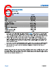


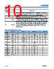


1. General Overview & Package (BGA)
️· Package: It's a Ball Grid Array (BGA) package.
️· Pinout: The document provides a detailed pinout table for the BGA package (A1-G7). This table maps pin IDs to functions.
️· Multiple Channels: The LTM4640 appears to be a multi-channel (likely PolyPhase) switching regulator.
2. Power Input and Output Pins
️· VIN Pins (D3-D4, E3-E4, F4, G4): These are power input pins. They connect to the drain of the internal top MOSFETs. Input decoupling capacitors should be placed between these pins and GND.
️· VOUT Pins (A1-A4, F1-F3, G1-G3, A5-A7, G5-G7): These are power output pins. They form the output of the switching regulator. Output decoupling capacitance should be placed between these pins and GND.
️· GND Pins (B2, B6, C3-C7, D5-D7, E5-E7, F5-F7, G6-G7): These are ground pins. Use large PCB copper areas to connect these together.
3. Control & Configuration Pins
️· RUN (B4): Enables/disables the regulator. Above 1.35V enables, below 1.1V shuts down.
️· PGOOD (B5): An open-drain logic pin indicating power good status. Pulled low when the FB pin is out of tolerance.
️· FB (C1): Negative input to the error amplifier. Connected to VOSNS+ with a 10kΩ resistor. Sets the output voltage.
️· VOSNS+ (B1): Positive input to a differential remote sense amplifier. Connected to FB with a 10kΩ resistor.
️· VOSNS– (C2): Negative input to the remote sense amplifier. A resistor between FB and VOSNS– sets the output voltage.
️· COMPa (D1): Current control threshold and compensation point. Connect to COMPb for internal compensation, or to a Type-II C-R-C network for customized compensation.
️· MODE/CLKIN (D2): Selects continuous (FCM) or discontinuous (DCM) mode. Can also be used for external clock synchronization.
️· FREQ (E1): Adjusts the switching frequency. A resistor from this pin to GND increases the frequency, while a resistor to INTVCC decreases it.
️· TRACK/SS (E2): Output tracking and soft start. A capacitor on this pin provides soft-start functionality.
️· COMPb (F1): Connect to COMPa for internal compensation.
️· CLKOUT (F2): Output clock signal for PolyPhase operation. Phase relationship is determined by PHMODE.
️· PHMODE (G5): Selects phase relationship for PolyPhase operation (2, 3, or 4 phases).
4. Internal Voltage/Signal Pins
️· INTVCC (B3): Internal 3.3V regulator output. Powers internal drivers and control circuits.
️· SW (B7): Switching node for testing. Can be snubbered.
️· TSENSE+ (A6): Positive input to a temperature monitor.
️· TSENSE– (A7): Low-side of the internal temperature monitor.
️· MODE/CLKIN
️· FB
️· VOSNS+
️· VOSNS–
5. Important Notes & Functionality
️· PolyPhase Operation: The LTM4640 is designed for PolyPhase operation, allowing for multiple phases. FB and COMPa pins should be tied together in parallel operation.
️· Remote Sensing: Uses a differential remote sense amplifier to compensate for voltage drops on the output traces.
️· Soft Start: A capacitor on the TRACK/SS pin provides a soft-start function.
️· Discontinuous/Continuous Mode: Can operate in discontinuous (DCM) or continuous (FCM) mode, selectable via MODE/CLKIN.
️· Compensation: The regulator is internally compensated, but external compensation networks can be used.
1. General Overview & Package (BGA)
️· Package: It's a Ball Grid Array (BGA) package.
️· Pinout: The document provides a detailed pinout table for the BGA package (A1-G7). This table maps pin IDs to functions.
️· Multiple Channels: The LTM4640 appears to be a multi-channel (likely PolyPhase) switching regulator.
2. Power Input and Output Pins
️· VIN Pins (D3-D4, E3-E4, F4, G4): These are power input pins. They connect to the drain of the internal top MOSFETs. Input decoupling capacitors should be placed between these pins and GND.
️· VOUT Pins (A1-A4, F1-F3, G1-G3, A5-A7, G5-G7): These are power output pins. They form the output of the switching regulator. Output decoupling capacitance should be placed between these pins and GND.
️· GND Pins (B2, B6, C3-C7, D5-D7, E5-E7, F5-F7, G6-G7): These are ground pins. Use large PCB copper areas to connect these together.
3. Control & Configuration Pins
️· RUN (B4): Enables/disables the regulator. Above 1.35V enables, below 1.1V shuts down.
️· PGOOD (B5): An open-drain logic pin indicating power good status. Pulled low when the FB pin is out of tolerance.
️· FB (C1): Negative input to the error amplifier. Connected to VOSNS+ with a 10kΩ resistor. Sets the output voltage.
️· VOSNS+ (B1): Positive input to a differential remote sense amplifier. Connected to FB with a 10kΩ resistor.
️· VOSNS– (C2): Negative input to the remote sense amplifier. A resistor between FB and VOSNS– sets the output voltage.
️· COMPa (D1): Current control threshold and compensation point. Connect to COMPb for internal compensation, or to a Type-II C-R-C network for customized compensation.
️· MODE/CLKIN (D2): Selects continuous (FCM) or discontinuous (DCM) mode. Can also be used for external clock synchronization.
️· FREQ (E1): Adjusts the switching frequency. A resistor from this pin to GND increases the frequency, while a resistor to INTVCC decreases it.
️· TRACK/SS (E2): Output tracking and soft start. A capacitor on this pin provides soft-start functionality.
️· COMPb (F1): Connect to COMPa for internal compensation.
️· CLKOUT (F2): Output clock signal for PolyPhase operation. Phase relationship is determined by PHMODE.
️· PHMODE (G5): Selects phase relationship for PolyPhase operation (2, 3, or 4 phases).
4. Internal Voltage/Signal Pins
️· INTVCC (B3): Internal 3.3V regulator output. Powers internal drivers and control circuits.
️· SW (B7): Switching node for testing. Can be snubbered.
️· TSENSE+ (A6): Positive input to a temperature monitor.
️· TSENSE– (A7): Low-side of the internal temperature monitor.
️· MODE/CLKIN
️· FB
️· VOSNS+
️· VOSNS–
5. Important Notes & Functionality
️· PolyPhase Operation: The LTM4640 is designed for PolyPhase operation, allowing for multiple phases. FB and COMPa pins should be tied together in parallel operation.
️· Remote Sensing: Uses a differential remote sense amplifier to compensate for voltage drops on the output traces.
️· Soft Start: A capacitor on the TRACK/SS pin provides a soft-start function.
️· Discontinuous/Continuous Mode: Can operate in discontinuous (DCM) or continuous (FCM) mode, selectable via MODE/CLKIN.
️· Compensation: The regulator is internally compensated, but external compensation networks can be used.
| Part No. | LTM4650 |
| Manufacturer | AD |
| Size | 1Mb |
| Pages | 38 pages |
| Description | 20VIN, 20A Step-Down DC-to-DC μModule Regulator |
| ¿ALLDATASHEET es útil para Ud.? [ DONATE ] |
Todo acerca de Alldatasheet | Publicidad | Contáctenos | Política de Privacidad | Enlace a la hoja de datos | Intercambio de Enlaces | Lista de Fabricantes All Rights Reserved©Alldatasheet.com |
| Russian : Alldatasheetru.com | Korean : Alldatasheet.co.kr | Spanish : Alldatasheet.es | French : Alldatasheet.fr | Italian : Alldatasheetit.com Portuguese : Alldatasheetpt.com | Polish : Alldatasheet.pl | Vietnamese : Alldatasheet.vn Indian : Alldatasheet.in | Mexican : Alldatasheet.com.mx | British : Alldatasheet.co.uk | New Zealand : Alldatasheet.co.nz |
|
Family Site : ic2ic.com |
icmetro.com |
 Mexican ▼
  English
 Chinese
 German
 Japanese
 Russian
 Korean
 Spanish
 French
 Italian
 Portuguese
 Polish
 Vietnamese
 Indian
 British
 New Zealand