 |
Motor de Búsqueda de Datasheet de Componentes Electrónicos |
|
|
Motor de Búsqueda de Datasheet de Componentes Electrónicos |
|
The question interval is too short.
Please try again in a few seconds.

Hello, Please ask a question about ADRF6603ACPZ-R7 Datasheet
# Example questions:
➢ If an external lo signal is desired, what conditions must be met regarding the pll_en and lop/lon pins?
➢ What is the primary function of the ip3set pin, and how does it affect the device's performance?
➢ What are the required decoupling capacitors for the vcc1 pin, and why are they important?
| Part No. | ADRF6603ACPZ-R7 |
| Manufacturer | AD |
| Size | 504 Kbytes |
| Pages | 24 pages |
| Description | 2100 MHz to 2600 MHz Rx Mixer with Integrated Fractional-N PLL and VCO |









1. General Description:
️· The ADRF6603 is a highly integrated, low noise, voltage-controlled oscillator (VCO) with a mixer. It's designed for demanding RF applications, like those found in wireless infrastructure.
️· It can operate in either an internal VCO mode or use an external LO input.
️· It has a wide tuning range and good phase noise performance.
2. Key Features & Specifications:
️· Frequency Range: (Not explicitly mentioned in this extract, but implied by the LO and VCO capabilities.)
️· Operating Voltage: 4.75V to 5.25V (for several power supply pins like VCC1, VCC2, VCC_V2I).
️· Temperature Range: -40°C to +85°C (Operating), -65°C to +150°C (Storage)
️· LO Drive Enable (LODRV_EN): Controls whether the LO pins (LON, LOP) are inputs or outputs.
️· PLL Enable (PLL_EN): Switches between the internal PLL and external LO.
️· External LO Frequency: The external LO drive frequency must be 1× LO.
️· IIP3 Adjustment: Can be adjusted using a resistor connected to the IP3SET pin.
️· Exposed Paddle: Should be soldered to a low-impedance ground plane.
3. Pin Functions (Most Important):
️· VCCx: Power supply pins (require decoupling capacitors - 100pF and 0.1uF near the pin).
️· REF_IN: Reference input, nominal input level 1V p-p, range 12-160 MHz.
️· MUXOUT: Programmable output for reference or lock detect.
️· DATA/CLK/LE: Serial interface for programming registers and controlling the device.
️· LON/LOP: Local Oscillator Input/Output.
️· VTUNE: VCO Control Voltage Input (1.5V - 2.5V).
️· DECLx: Decoupling Nodes (require capacitors).
️· PLL_EN: Enables/Disables the internal PLL and selects between internal or external LO.
️· LODRV_EN: Enables/Disables LO output drivers.
4. Register Control (Implied):
️· Multiple registers are used for configuring the ADRF6603.
️· Register 4 controls the charge pump current.
️· Register 5 includes bits (DB6 - PLEN, DB3 - LDRV) that affect the PLL and LO driver functions.
️· Serial data is loaded MSB first.
5. Thermal Considerations:
️· Maximum junction temperature is 150°C.
️· θJA (thermal resistance junction-to-ambient) is 35°C/W. This implies good heat sinking is important.
IMPORTANT NOTES (PLEASE READ):
️· This is a partial datasheet extract. It *does not* contain all the information necessary to use the ADRF6603 correctly. You *must* refer to the full datasheet for detailed specifications, register descriptions, timing diagrams, application circuits, and other critical information.
️· Voltage levels and timings: Always refer to the datasheet for precise voltage levels, timing requirements, and any recommended external components.
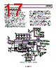
️· Application Circuits: The datasheet will contain example application circuits that show how to connect and use the ADRF6603 in a real-world system. These circuits are essential for optimal performance.
️· Decoupling: Proper decoupling capacitors are crucial for stable operation. The datasheet specifies these capacitors for each power pin.
️· Ground Plane: The exposed paddle *must* be connected to a low-impedance ground plane.
1. General Description:
️· The ADRF6603 is a highly integrated, low noise, voltage-controlled oscillator (VCO) with a mixer. It's designed for demanding RF applications, like those found in wireless infrastructure.
️· It can operate in either an internal VCO mode or use an external LO input.
️· It has a wide tuning range and good phase noise performance.
2. Key Features & Specifications:
️· Frequency Range: (Not explicitly mentioned in this extract, but implied by the LO and VCO capabilities.)
️· Operating Voltage: 4.75V to 5.25V (for several power supply pins like VCC1, VCC2, VCC_V2I).
️· Temperature Range: -40°C to +85°C (Operating), -65°C to +150°C (Storage)
️· LO Drive Enable (LODRV_EN): Controls whether the LO pins (LON, LOP) are inputs or outputs.
️· PLL Enable (PLL_EN): Switches between the internal PLL and external LO.
️· External LO Frequency: The external LO drive frequency must be 1× LO.
️· IIP3 Adjustment: Can be adjusted using a resistor connected to the IP3SET pin.
️· Exposed Paddle: Should be soldered to a low-impedance ground plane.
3. Pin Functions (Most Important):
️· VCCx: Power supply pins (require decoupling capacitors - 100pF and 0.1uF near the pin).
️· REF_IN: Reference input, nominal input level 1V p-p, range 12-160 MHz.
️· MUXOUT: Programmable output for reference or lock detect.
️· DATA/CLK/LE: Serial interface for programming registers and controlling the device.
️· LON/LOP: Local Oscillator Input/Output.
️· VTUNE: VCO Control Voltage Input (1.5V - 2.5V).
️· DECLx: Decoupling Nodes (require capacitors).
️· PLL_EN: Enables/Disables the internal PLL and selects between internal or external LO.
️· LODRV_EN: Enables/Disables LO output drivers.
4. Register Control (Implied):
️· Multiple registers are used for configuring the ADRF6603.
️· Register 4 controls the charge pump current.
️· Register 5 includes bits (DB6 - PLEN, DB3 - LDRV) that affect the PLL and LO driver functions.
️· Serial data is loaded MSB first.
5. Thermal Considerations:
️· Maximum junction temperature is 150°C.
️· θJA (thermal resistance junction-to-ambient) is 35°C/W. This implies good heat sinking is important.
IMPORTANT NOTES (PLEASE READ):
️· This is a partial datasheet extract. It *does not* contain all the information necessary to use the ADRF6603 correctly. You *must* refer to the full datasheet for detailed specifications, register descriptions, timing diagrams, application circuits, and other critical information.
️· Voltage levels and timings: Always refer to the datasheet for precise voltage levels, timing requirements, and any recommended external components.
️· Application Circuits: The datasheet will contain example application circuits that show how to connect and use the ADRF6603 in a real-world system. These circuits are essential for optimal performance.
️· Decoupling: Proper decoupling capacitors are crucial for stable operation. The datasheet specifies these capacitors for each power pin.
️· Ground Plane: The exposed paddle *must* be connected to a low-impedance ground plane.
| Part No. | ADRF6603ACPZ-R7 |
| Manufacturer | AD |
| Size | 504 Kbytes |
| Pages | 24 pages |
| Description | 2100 MHz to 2600 MHz Rx Mixer with Integrated Fractional-N PLL and VCO |
| ¿ALLDATASHEET es útil para Ud.? [ DONATE ] |
Todo acerca de Alldatasheet | Publicidad | Contáctenos | Política de Privacidad | Enlace a la hoja de datos | Intercambio de Enlaces | Lista de Fabricantes All Rights Reserved©Alldatasheet.com |
| Russian : Alldatasheetru.com | Korean : Alldatasheet.co.kr | Spanish : Alldatasheet.es | French : Alldatasheet.fr | Italian : Alldatasheetit.com Portuguese : Alldatasheetpt.com | Polish : Alldatasheet.pl | Vietnamese : Alldatasheet.vn Indian : Alldatasheet.in | Mexican : Alldatasheet.com.mx | British : Alldatasheet.co.uk | New Zealand : Alldatasheet.co.nz |
|
Family Site : ic2ic.com |
icmetro.com |
 Mexican ▼
  English
 Chinese
 German
 Japanese
 Russian
 Korean
 Spanish
 French
 Italian
 Portuguese
 Polish
 Vietnamese
 Indian
 British
 New Zealand