|
Motor de Búsqueda de Datasheet de Componentes Electrónicos |
|
|
Motor de Búsqueda de Datasheet de Componentes Electrónicos |
|
ADRF6603ACPZ-R7 Datasheet(PDF) 8 Page - Analog Devices |
|
|
|||||||||||||||||||||||||||||
ADRF6603ACPZ-R7 Datasheet(HTML) 8 Page - Analog Devices |
|
|
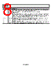
8 / 24 page  ADRF6603 Rev. 0 | Page 8 of 24 Pin No. Mnemonic Description 27 VCC_V2I Power Supply. Power supply voltage range is 4.75 V to 5.25 V. Each power supply pin should be decoupled with a 100 pF capacitor and a 0.1 μF capacitor located close to the pin. 29 IP3SET Connect a resistor from this pin to a +5 V supply to adjust IIP3. Normally leave open. 32, 33 NC No Connection. 36 LODRV_EN LO Driver Enable. Together with Pin 16 (PLL_EN), this digital input pin determines whether the LOP and LON pins operate as inputs or outputs. LOP and LON become inputs if the PLL_EN pin is low or if the PLL_EN pin is set high with the PLEN bit (DB6 in Register 5) set to 0. LOP and LON become outputs if either the LODRV_EN pin or the LDRV bit (DB3 in Register 5) is set to 1 while the PLL_EN pin is set high. The external LO drive frequency must be 1× LO. This pin should not be left floating. 37, 38 LON, LOP Local Oscillator Input/Output. The internally generated 1× LO is available on these pins. When internal LO generation is disabled, an external 1× LO can be applied to these pins. 39 VTUNE VCO Control Voltage Input. This pin is driven by the output of the loop filter. The nominal input voltage range on this pin is 1.5 V to 2.5 V. 40 DECLVCO Decoupling Node for VCO LDO. Connect a 100 pF capacitor and a 10 μF capacitor between this pin and ground. EP EPAD Exposed Paddle. The exposed paddle should be soldered to a low impedance ground plane. |
|
|
Enlace URL |
| ¿ALLDATASHEET es útil para Ud.? [ DONATE ] |
Todo acerca de Alldatasheet | Publicidad | Contáctenos | Política de Privacidad | Enlace a la hoja de datos | Intercambio de Enlaces | Lista de Fabricantes All Rights Reserved©Alldatasheet.com |
| Russian : Alldatasheetru.com | Korean : Alldatasheet.co.kr | Spanish : Alldatasheet.es | French : Alldatasheet.fr | Italian : Alldatasheetit.com Portuguese : Alldatasheetpt.com | Polish : Alldatasheet.pl | Vietnamese : Alldatasheet.vn Indian : Alldatasheet.in | Mexican : Alldatasheet.com.mx | British : Alldatasheet.co.uk | New Zealand : Alldatasheet.co.nz |
|
Family Site : ic2ic.com |
icmetro.com |
 Mexican ▼
 English
 Chinese
 German
 Japanese
 Russian
 Korean
 Spanish
 French
 Italian
 Portuguese
 Polish
 Vietnamese
 Indian
 Mexican
 British
 New Zealand