 |
Motor de Búsqueda de Datasheet de Componentes Electrónicos |
|
|
Motor de Búsqueda de Datasheet de Componentes Electrónicos |
|
The question interval is too short.
Please try again in a few seconds.

Hello, Please ask a question about AD7013 Datasheet
# Example questions:
➢ What is the purpose of the load circuit described in figure 1, and why is it important when interpreting the timing characteristics for the digital outputs?
➢ What is the purpose of cr10 in relation to the rxclk signal, and how does changing its value affect the sampling rate?
➢ What is the relationship between mclk, dxclk, and rxclk? explain the signal flow and dependencies.
| Part No. | AD7013 |
| Manufacturer | AD |
| Size | 591 Kbytes |
| Pages | 20 pages |
| Description | CMOS TIA IS-54 Baseband Receive Port |






1. Device Overview (Implied)
️· The AD7013 is a device likely used for receiving and processing radio signals (or similar).
️· It's designed for use with a clock signal (MCLK) and relies heavily on timing parameters.
️· It has features for offset autocalibration in the receiver.
️· It supports different sampling rates for receiving data.
2. Timing Characteristics (Most Important Section)
The document provides extensive timing characteristics, broken down into three main areas:
️· Serial Interface Timing (Figure 2 & 3)
- MCLK & DxCLK Relationship: MCLK (Master Clock) is used to generate DxCLK (Data Clock). Timing parameters define the delays and durations of these signals.
- Data Transfer: This section details the timing for writing to the AD7013’s internal registers using a serial interface.
- Parameters: Includes: MCLK Cycle Time, MCLK High/Low Time, Propagation Delays, Setup/Hold Times for DATA IN and FRAME IN signals.
️· Receive Section Timing (Figure 5)
- Sampling Rates: The AD7013 supports different sampling rates (4x and 2x the symbol rate) controlled by a CR10 setting. This affects RxCLK timing.
- Parameters: Includes: Power-up time, Propagation Delays, Cycle Times, Setup/Hold Times for RxCLK and RxFRAME signals.
- 3-State Control: The device supports 3-state control for the receiver channel.
️· Timing Definitions (General)
- `t1`: A fundamental time unit used to derive other timing parameters. This is critical.
- Setup and Hold Times: Critical for reliable data transfer. These define the minimum time data must be stable before and after a clock edge.
- Propagation Delays: The time it takes for a signal to propagate through the device.
- Cycle Times: The duration of a signal's period (high and low states).
3. Figures Explained
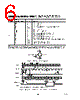
️· Figure 1: Illustrates a load circuit used for measuring timing parameters. It’s relevant for understanding how the timing specs are derived.
️· Figure 2: Serial Interface Timing Diagram (4x Sampling Rate).
️· Figure 3: Serial Interface Timing Diagram (2x Sampling Rate).
️· Figure 5: Illustrates 3-State Timing for the Receiver channel.
4. Key Parameters and Their Importance
️· t1: The base time unit. Knowing its value is essential for calculating all other timing parameters.
️· CR10 Setting: Controls the sampling rate (directly affects RxCLK timing).
️· CR13 Setting: Enables or disables offset autocalibration in the receiver.
️· Setup and Hold Times: Absolutely crucial for data integrity. Insufficient setup or hold time will lead to data corruption.
️· Propagation Delays: Determine the maximum data transfer speed.
5. Important Notes/Caveats in the Document
️· Temperature Dependence: Timing parameters are specified at a particular temperature. They will vary with temperature.
️· Load Circuit: The timing measurements are taken with a specific load circuit (Figure 1). External circuitry might affect the results.
️· Fundamental Time Unit (t1): The document implies this is a known or derived value; the actual value of `t1` is not provided.
️· Device Relinquish Time: This refers to the time taken for the receiver to go from a valid state to a high-impedance (3-state) state.
️· 3-State Control: This allows the receiver to be put in a high impedance state to avoid interference.
VERY IMPORTANT CAVEATS & DISCLAIMERS
1. Extensive Detail: This documentation is incredibly detailed and is intended for experienced engineers familiar with radio frequency (RF) receiver design and signal processing.
2. Missing Information: The document *does not* include the specific value of `t1`. This is vital to interpret all of the timing specs.
3. Context is Crucial: These timing specifications only make sense within the context of the entire AD7013 datasheet and application note.
4. Consult the Complete Datasheet: This is a *snippet* of documentation. The full datasheet and relevant application notes are absolutely necessary for proper device operation.
5. Application-Specific: The timing requirements of your application will dictate whether or not the AD7013 is suitable and whether these timing parameters can be met.
6. Design Considerations: Careful consideration must be given to the layout and routing of signals on the printed circuit board (PCB) to minimize signal reflections and ensure proper impedance matching.
1. Device Overview (Implied)
️· The AD7013 is a device likely used for receiving and processing radio signals (or similar).
️· It's designed for use with a clock signal (MCLK) and relies heavily on timing parameters.
️· It has features for offset autocalibration in the receiver.
️· It supports different sampling rates for receiving data.
2. Timing Characteristics (Most Important Section)
The document provides extensive timing characteristics, broken down into three main areas:
️· Serial Interface Timing (Figure 2 & 3)
- MCLK & DxCLK Relationship: MCLK (Master Clock) is used to generate DxCLK (Data Clock). Timing parameters define the delays and durations of these signals.
- Data Transfer: This section details the timing for writing to the AD7013’s internal registers using a serial interface.
- Parameters: Includes: MCLK Cycle Time, MCLK High/Low Time, Propagation Delays, Setup/Hold Times for DATA IN and FRAME IN signals.
️· Receive Section Timing (Figure 5)
- Sampling Rates: The AD7013 supports different sampling rates (4x and 2x the symbol rate) controlled by a CR10 setting. This affects RxCLK timing.
- Parameters: Includes: Power-up time, Propagation Delays, Cycle Times, Setup/Hold Times for RxCLK and RxFRAME signals.
- 3-State Control: The device supports 3-state control for the receiver channel.
️· Timing Definitions (General)
- `t1`: A fundamental time unit used to derive other timing parameters. This is critical.
- Setup and Hold Times: Critical for reliable data transfer. These define the minimum time data must be stable before and after a clock edge.
- Propagation Delays: The time it takes for a signal to propagate through the device.
- Cycle Times: The duration of a signal's period (high and low states).
3. Figures Explained
️· Figure 1: Illustrates a load circuit used for measuring timing parameters. It’s relevant for understanding how the timing specs are derived.
️· Figure 2: Serial Interface Timing Diagram (4x Sampling Rate).
️· Figure 3: Serial Interface Timing Diagram (2x Sampling Rate).
️· Figure 5: Illustrates 3-State Timing for the Receiver channel.
4. Key Parameters and Their Importance
️· t1: The base time unit. Knowing its value is essential for calculating all other timing parameters.
️· CR10 Setting: Controls the sampling rate (directly affects RxCLK timing).
️· CR13 Setting: Enables or disables offset autocalibration in the receiver.
️· Setup and Hold Times: Absolutely crucial for data integrity. Insufficient setup or hold time will lead to data corruption.
️· Propagation Delays: Determine the maximum data transfer speed.
5. Important Notes/Caveats in the Document
️· Temperature Dependence: Timing parameters are specified at a particular temperature. They will vary with temperature.
️· Load Circuit: The timing measurements are taken with a specific load circuit (Figure 1). External circuitry might affect the results.
️· Fundamental Time Unit (t1): The document implies this is a known or derived value; the actual value of `t1` is not provided.
️· Device Relinquish Time: This refers to the time taken for the receiver to go from a valid state to a high-impedance (3-state) state.
️· 3-State Control: This allows the receiver to be put in a high impedance state to avoid interference.
VERY IMPORTANT CAVEATS & DISCLAIMERS
1. Extensive Detail: This documentation is incredibly detailed and is intended for experienced engineers familiar with radio frequency (RF) receiver design and signal processing.
2. Missing Information: The document *does not* include the specific value of `t1`. This is vital to interpret all of the timing specs.
3. Context is Crucial: These timing specifications only make sense within the context of the entire AD7013 datasheet and application note.
4. Consult the Complete Datasheet: This is a *snippet* of documentation. The full datasheet and relevant application notes are absolutely necessary for proper device operation.
5. Application-Specific: The timing requirements of your application will dictate whether or not the AD7013 is suitable and whether these timing parameters can be met.
6. Design Considerations: Careful consideration must be given to the layout and routing of signals on the printed circuit board (PCB) to minimize signal reflections and ensure proper impedance matching.
| Part No. | AD7013 |
| Manufacturer | AD |
| Size | 591 Kbytes |
| Pages | 20 pages |
| Description | CMOS TIA IS-54 Baseband Receive Port |
| ¿ALLDATASHEET es útil para Ud.? [ DONATE ] |
Todo acerca de Alldatasheet | Publicidad | Contáctenos | Política de Privacidad | Enlace a la hoja de datos | Intercambio de Enlaces | Lista de Fabricantes All Rights Reserved©Alldatasheet.com |
| Russian : Alldatasheetru.com | Korean : Alldatasheet.co.kr | Spanish : Alldatasheet.es | French : Alldatasheet.fr | Italian : Alldatasheetit.com Portuguese : Alldatasheetpt.com | Polish : Alldatasheet.pl | Vietnamese : Alldatasheet.vn Indian : Alldatasheet.in | Mexican : Alldatasheet.com.mx | British : Alldatasheet.co.uk | New Zealand : Alldatasheet.co.nz |
|
Family Site : ic2ic.com |
icmetro.com |
 Mexican ▼
  English
 Chinese
 German
 Japanese
 Russian
 Korean
 Spanish
 French
 Italian
 Portuguese
 Polish
 Vietnamese
 Indian
 British
 New Zealand