|
Motor de Búsqueda de Datasheet de Componentes Electrónicos |
|
|
Motor de Búsqueda de Datasheet de Componentes Electrónicos |
|
9601-11 Datasheet(PDF) 7 Page - Peregrine Semiconductor Corp. |
|
|
|||||||||||||||||||||||||||||
9601-11 Datasheet(HTML) 7 Page - Peregrine Semiconductor Corp. |
|
|
7 / 14 page 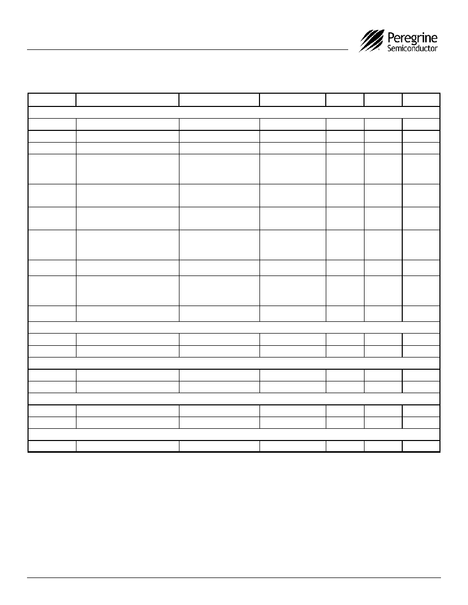 Product Specification PE9601 Page 7 of 14 Document No. 70-0025-05 │ www.psemi.com ©2005 Peregrine Semiconductor Corp. All rights reserved. Table 6. AC Characteristics VDD = 3.0 V, -40° C < TA < 85° C, unless otherwise specified Symbol Parameter Test Program Name Conditions Min Max Units Control Interface and Latches (see Figure 5 and Figure 6) fClk Serial data clock frequency (Note 1) 10 MHz tClkH Serial clock HIGH time t_clk_H (s) 30 ns tClkL Serial clock LOW time t_clk_L (s) 30 ns tDSU Sdata set-up time after Sclk rising edge, D[7:0] set-up time to M1_WR, M2_WR, A_WR, E_WR rising edge t_dsu_”xxx” (s) where “xxx” is name of pin being tested 10 ns tDHLD Sdata hold time after Sclk rising edge, D[7:0] hold time to M1_WR, M2_WR, A_WR rising edge t_dhid_”xxx” (s) where “xxx” is name of pin being tested 10 ns tPW S_WR, M1_WR, M2_WR, A_WR, E_WR pulse width t_pw_”xxx” (s) where “xxx” is name of pin being tested 30 ns tCWR Sclk rising edge to S_WR rising edge. S_WR, M1_WR, M2_WR, A_WR falling edge to Hop_WR rising edge t_cwr_”xxx” (s) where “xxx” is name of pin being tested 30 ns tCE Sclk falling edge to E_WR transition t_ce (s) 30 ns tWRC S_WR falling edge to Sclk rising edge. Hop_WR falling edge to S_WR, M1_WR, M2_WR, A_WR rising edge t_wrc_”xxx” (s) where “xxx” is name of pin being tested 30 ns tEC E_WR transition to Sclk rising edge t_ec (s) 30 ns Main Divider (Including Prescaler) Fin Operating frequency RF_sens 200 2200 MHz PFin Input level range RF_sens External AC coupling 0 5 dBm Main Divider (Prescaler Bypassed) Fin Operating frequency 20 220 MHz PFin Input level range External AC coupling -5 5 dBm Reference Divider fr Operating frequency Fc_sens (Note 3) 100 MHz Pfr Reference input power (Note 2) Fc_sens Single ended input -2 dBm Phase Detector fc Comparison frequency (Note 3) 20 MHz Note 1: Fclk is verified during the functional pattern test. Serial programming sections of the functional pattern are clocked at 10 MHz to verify Fclk specification. Note 2: CMOS logic levels can be used to drive reference input if DC coupled. Voltage input needs to be a minimum of 0.5Vp-p. Note 3: Parameter is guaranteed through characterization only and is not tested. |
|
|
Enlace URL |
| ¿ALLDATASHEET es útil para Ud.? [ DONATE ] |
Todo acerca de Alldatasheet | Publicidad | Contáctenos | Política de Privacidad | Enlace a la hoja de datos | Intercambio de Enlaces | Lista de Fabricantes All Rights Reserved©Alldatasheet.com |
| Russian : Alldatasheetru.com | Korean : Alldatasheet.co.kr | Spanish : Alldatasheet.es | French : Alldatasheet.fr | Italian : Alldatasheetit.com Portuguese : Alldatasheetpt.com | Polish : Alldatasheet.pl | Vietnamese : Alldatasheet.vn Indian : Alldatasheet.in | Mexican : Alldatasheet.com.mx | British : Alldatasheet.co.uk | New Zealand : Alldatasheet.co.nz |
|
Family Site : ic2ic.com |
icmetro.com |
 Mexican ▼
 English
 Chinese
 German
 Japanese
 Russian
 Korean
 Spanish
 French
 Italian
 Portuguese
 Polish
 Vietnamese
 Indian
 Mexican
 British
 New Zealand