|
Motor de Búsqueda de Datasheet de Componentes Electrónicos |
|
|
Motor de Búsqueda de Datasheet de Componentes Electrónicos |
|
LTM4650 Datasheet(PDF) 12 Page - Analog Devices |
|
|
|||||||||||||||||||||||||||||
LTM4650 Datasheet(HTML) 12 Page - Analog Devices |
|
|
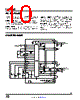
12 / 28 page  LTM4660 12 Rev. 0 For more information www.analog.com FAULT TIMER TRACK/SS 0V 0.5V 1.2V 4V FAULT TIMER TRACK/SS 0V 0.5V 1.2V (a) Balancing Completed within One Timer Period (b) More Than One Timer Period 4660 F01 Figure 1. Charge Balancing During Power-Up FAULT TIMER 0.5V 1.2V TRACK/SS FAULT TIMER TRACK/SS 4660 F02 0.5V 1.2V (a) Balancing Completed within One Timer Period (b) More Than One Timer Period Figure 2. Charge Balancing During Normal Operation OPERATION not be pulled low during this initial power up. If the volt- ages across CFLY and CMID reach VIN/2 before the TIMER capacitor’s voltage reaches 1.2V, the TRACK/SS will be released and allowed to charge up. The TIMER pin will reset to ground and remain there. Normal operation will begin (see Figure 1a). If, however, the CFLY or CMID voltage is not at VIN/2 when VTIMER reaches 1.2V, the internal current sources will be turned OFF and the TIMER capacitor will be charged at half the initial rate until it reaches 4V. Timer will then be reset to zero, and the LTM4660 will repeat the above process again until CFLY and CMID are at VIN/2. (See Figure 1b). During normal operation, only CMID is monitored for deviation away from VIN/2 by a window amount set by a resistor connected from HYS_PRGM to ground. The voltage across this resistor sets the same amount of win- dow threshold above and below VIN/2. If VCMID leaves this voltage window, all switching will stop, and the TRACK/ SS pin will be pulled low. Corresponding internal current sources will be turned on to bring CFLY and CMID voltages back to VIN/2. FAULT will be pulled low and released once the balancing is complete. During this balancing period, PGOOD will also be pulled low. The TRACK/SS pin is also allowed to charge up upon the completion of balancing (see Figure 2). Connecting HYS_PRGM to INTVCC sets the window threshold to ±0.8V around VIN/2. Main Control Loop Once the capacitor balancing phase is complete, nor- mal operation begins. Power switches are turned ON/ OFF based on peak current in the power inductor. Peak inductor current is controlled by voltage on COMPa pin, which is the output of a transconductance error amplifier. The VFB pin receives the voltage feedback signal from VOUT, which is compared to the internal reference volt- age by the error amplifier. When load current increases, it causes a slight decrease in VFB relative to the 0.8V refer- ence voltage, which in turn causes the COMPa voltage to increase until average inductor current matches the new load current. During each switching cycle, capacitor CFLY is connected in series with or parallel to CMID. Voltage at C+ alternates between VIN and VIN/2 whereas voltage at C– alternates between VIN/2 and ground. The voltage at MID and across CFLY will each be approximately at VIN/2. |
|
Enlace URL |
| ¿ALLDATASHEET es útil para Ud.? [ DONATE ] |
Todo acerca de Alldatasheet | Publicidad | Contáctenos | Política de Privacidad | Enlace a la hoja de datos | Intercambio de Enlaces | Lista de Fabricantes All Rights Reserved©Alldatasheet.com |
| Russian : Alldatasheetru.com | Korean : Alldatasheet.co.kr | Spanish : Alldatasheet.es | French : Alldatasheet.fr | Italian : Alldatasheetit.com Portuguese : Alldatasheetpt.com | Polish : Alldatasheet.pl | Vietnamese : Alldatasheet.vn Indian : Alldatasheet.in | Mexican : Alldatasheet.com.mx | British : Alldatasheet.co.uk | New Zealand : Alldatasheet.co.nz |
|
Family Site : ic2ic.com |
icmetro.com |
 Mexican ▼
 English
 Chinese
 German
 Japanese
 Russian
 Korean
 Spanish
 French
 Italian
 Portuguese
 Polish
 Vietnamese
 Indian
 Mexican
 British
 New Zealand