|
Motor de Búsqueda de Datasheet de Componentes Electrónicos |
|
|
Motor de Búsqueda de Datasheet de Componentes Electrónicos |
|
ICS9148-36 Datasheet(PDF) 9 Page - Integrated Device Technology |
|
|
|||||||||||||||||||||||||||||
ICS9148-36 Datasheet(HTML) 9 Page - Integrated Device Technology |
|
|
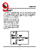
9 / 16 page  9 ICS9148-36 Pins 2, 7, 8, 25 & 26 on the ICS9148-36 serve as dual signal functions to the device. During initial power-up, they act as input pins. The logic level (voltage) that is present on these pins at this time is read and stored into a 4-bit internal data latch. At the end of Power-On reset, (see AC characteristics for timing values), the device changes the mode of operations for these pins to an output function. In this mode the pins produce the specified buffered clocks to external loads. To program (load) the internal configuration register for these pins, a resistor is connected to either the VDD (logic 1) power supply or the GND (logic 0) voltage potential. A 10 Kilohm(10K) resistor is used to provide both the solid CMOS programming voltage needed during the power-up programming period and to provide an insignificant load on the output clock during the subsequent operating period. Figs. 1 and 2 show the recommended means of implementing this function. In Fig. 1 either one of the resistors is loaded onto the board (selective stuffing) to configure the devices internal logic. Figs. 2a and b provide a single resistor loading option where either solder spot tabs or a physical jumper header may be used. Shared Pin Operation - Input/Output Pins Fig. 1 These figures illustrate the optimal PCB physical layout options. These configuration resistors are of such a large ohmic value that they do not effect the low impedance clock signals. The layouts have been optimized to provide as little impedance transition to the clock signal as possible, as it passes through the programming resistor pad(s). |
|
|
Enlace URL |
| ¿ALLDATASHEET es útil para Ud.? [ DONATE ] |
Todo acerca de Alldatasheet | Publicidad | Contáctenos | Política de Privacidad | Enlace a la hoja de datos | Intercambio de Enlaces | Lista de Fabricantes All Rights Reserved©Alldatasheet.com |
| Russian : Alldatasheetru.com | Korean : Alldatasheet.co.kr | Spanish : Alldatasheet.es | French : Alldatasheet.fr | Italian : Alldatasheetit.com Portuguese : Alldatasheetpt.com | Polish : Alldatasheet.pl | Vietnamese : Alldatasheet.vn Indian : Alldatasheet.in | Mexican : Alldatasheet.com.mx | British : Alldatasheet.co.uk | New Zealand : Alldatasheet.co.nz |
|
Family Site : ic2ic.com |
icmetro.com |
 Mexican ▼
 English
 Chinese
 German
 Japanese
 Russian
 Korean
 Spanish
 French
 Italian
 Portuguese
 Polish
 Vietnamese
 Indian
 Mexican
 British
 New Zealand