|
Motor de Búsqueda de Datasheet de Componentes Electrónicos |
|
|
Motor de Búsqueda de Datasheet de Componentes Electrónicos |
|
AMP01AX/883C Datasheet(PDF) 15 Page - Analog Devices |
|
|
|||||||||||||||||||||||||||||
AMP01AX/883C Datasheet(HTML) 15 Page - Analog Devices |
|
|
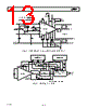
15 / 22 page  AMP01 –15– REV. D HEATSINKING To maintain high reliability, the die temperature of any IC should be kept as low as practicable, preferably below 100 °C. Although most AMP01 application circuits will produce very little internal heat — little more than the quiescent dissipation of 90 mW—some circuits will raise that to several hundred milliwatts (for example, the 4-20 mA current transmitter appli- cation, Figure 37). Excessive dissipation will cause thermal shutdown of the output stage thus protecting the device from damage. A heatsink is recommended in power applications to reduce the die temperature. Several appropriate heatsinks are available; the Thermalloy 6010B is especially easy to use and is inexpensive. Intended for dual-in-line packages, the heatsink may be attached with a cyanoacrylate adhesive. This heatsink reduces the thermal resis- tance between the junction and ambient environment to ap- proximately 80 °C/W. Junction (die) temperature can then be calculated by using the relationship: Pd = T J – T A θ JA where TJ and TA are the junction and ambient temperatures respectively, θ JA is the thermal resistance from junction to ambi- ent, and Pd is the device’s internal dissipation. OVERVOLTAGE PROTECTION Instrumentation amplifiers invariably sit at the front end of instrumentation systems where there is a high probability of exposure to overloads. Voltage transients, failure of a trans- ducer, or removal of the amplifier power supply while the signal source is connected may destroy or degrade the performance of an unprotected amplifier. Although it is impractical to protect an IC internally against connection to power lines, it is relatively easy to provide protection against typical system overloads. The AMP01 is internally protected against overloads for gains of up to 100. At higher gains, the protection is reduced and some external measures may be required. Limited internal over- load protection is used so that noise performance would not be significantly degraded. AMP01 noise level approaches the theoretical noise floor of the input stage which would be 4 nV/ √Hz at 1 kHz when the gain is set at 1000. Noise is the result of shot noise in the input devices and Johnson noise in the resistors. Resistor noise is calculated from the values of RG (200 Ω at a gain of 1000) and the input protection resistors (250 Ω). Active loads for the input transis- tors contribute less than 1 nV/ √Hz of noise. The measured noise level is typically 5 nV/ √Hz. Diodes across the input transistor’s base-emitter junctions, combined with 250 Ω input resistors and R G, protect against differential inputs of up to ±20 V for gains of up to 100. The diodes also prevent avalanche breakdown that would degrade the IB and IOS specifications. Decreasing the value of RG for gains above 100 limits the maximum input overload protection to ±10 V. External series resistors could be added to guard against higher voltage levels at the input, but resistors alone increase the input noise and degrade the signal-to-noise ratio, especially at high gains. Protection can also be achieved by connecting back-to-back 9.1 V Zener diodes across the differential inputs. This technique does not affect the input noise level and can be used down to a gain of 2 with minimal increase in input current. Although voltage-clamping elements look like short circuits at the limiting voltage, the majority of signal sources provide less than 50 mA, producing power levels that are easily handled by low-power Zeners. Simultaneous connection of the differential inputs to a low impedance signal above 10 V during normal circuit operation is unlikely. However, additional protection involves adding 100 Ω current-limiting resistors in each signal path prior to the voltage clamp, the resistors increase the input noise level to just 5.4 nV/ √Hz (refer to Figure 35). Input components, whether multiplexers or resistors, should be carefully selected to prevent the formation of thermocouple junctions that would degrade the input signal. VOUT +15V +IN –IN AMP01 9.1V 1W ZENERS 100 1W * 100 1W * OPTIONAL PROTECTION RESISTORS, SEE TEXT. * LINEAR INPUT RANGE, 5V MAXIMUM DIFFERENTIAL PROTECTION TO 30V –15V Figure 35. Input Overvoltage Protection for Gains 2 to 10,000 POWER SUPPLY CONSIDERATIONS Achieving the rated performance of precision amplifiers in a practical circuit requires careful attention to external influences. For example, supply noise and changes in the nominal voltage directly affect the input offset voltage. A PSR of 80 dB means that a change of 100 mV on the supply, not an uncommon value, will produce a 10 µV input offset change. Consequently, care should be taken in choosing a power unit that has a low output noise level, good line and load regulation, and good temperature stability. |
|
|
Enlace URL |
| ¿ALLDATASHEET es útil para Ud.? [ DONATE ] |
Todo acerca de Alldatasheet | Publicidad | Contáctenos | Política de Privacidad | Enlace a la hoja de datos | Intercambio de Enlaces | Lista de Fabricantes All Rights Reserved©Alldatasheet.com |
| Russian : Alldatasheetru.com | Korean : Alldatasheet.co.kr | Spanish : Alldatasheet.es | French : Alldatasheet.fr | Italian : Alldatasheetit.com Portuguese : Alldatasheetpt.com | Polish : Alldatasheet.pl | Vietnamese : Alldatasheet.vn Indian : Alldatasheet.in | Mexican : Alldatasheet.com.mx | British : Alldatasheet.co.uk | New Zealand : Alldatasheet.co.nz |
|
Family Site : ic2ic.com |
icmetro.com |
 Mexican ▼
 English
 Chinese
 German
 Japanese
 Russian
 Korean
 Spanish
 French
 Italian
 Portuguese
 Polish
 Vietnamese
 Indian
 Mexican
 British
 New Zealand